 ChipApex | Global Electronic Components Supplier

SEARCH
Search Product
Search Post
— IC芯片 | 连接器 | 传感器 | 被动器件 —
Search productSearch post
— IC芯片 | 连接器 | 传感器 | 被动器件 —
Consult the customer manager about the wholesale price.
consultation hotline:86-132-6715-2157
email:[email protected]
Contact the product manager for consultation. One-stop consultation is available.
Do you want a lower wholesale price? Please send us your inquiry and we will reply immediately.
IDT74FCT16500ATPVG is listed in the Universal Bus Functions range at ChipApex. The manufacturer field lists Renesas Electronics Corporation. Its product description is IC UNIV BUS TXRX 18BIT 56SSOP. Review the specifications below when checking this part for your BOM.
The IDT74FCT16500ATPVG is an 18-bit registered bus transceiver manufactured by Renesas Electronics Corporation. It operates within a 5V ±10% power supply range and supports an industrial temperature range of -40°C to +85°C. The device utilizes 0.5 micron CMOS technology, providing high-speed performance with typical output skew of 0.5 ns and maximum clock frequencies up to 150 MHz. It features independent control for each direction via dedicated output-enable, latch enable, and clock inputs.
Verify the specific suffix 'PVG' corresponds to the Shrink Small Outline Package (SSOP) variant as defined in the ordering information. Confirm that the 'A' designation aligns with the specified industrial temperature range (-40°C to +85°C). Ensure compliance with RoHS requirements if applicable, noting that older manufacturing runs may differ from current specifications.
Select this component when an 18-bit bidirectional registered interface is required with high drive strength. It serves as a replacement for ABT functions while offering lower power consumption. Consider the SSOP package constraints and verify that the 5V logic levels match the system voltage requirements. The independent control signals allow flexible configuration for various data transfer protocols.
This device belongs to the FCT family of Fast CMOS logic components. It is part of the 16-bit and 18-bit registered transceiver series designed for high-density digital systems. The product line emphasizes speed and low power dissipation, making it suitable for complex communication interfaces where data integrity and timing precision are critical.
Direct substitutes include other 18-bit registered transceivers from the same FCT family or compatible ABT-series devices. Verify pin compatibility and electrical characteristics such as drive current and propagation delay before substitution.
Data flow in each direction is controlled independently by separate output-enable, latch enable, and clock inputs, allowing simultaneous but distinct operations between ports A and B.
The power-off disable capability ensures that outputs remain in a high-impedance state when VCC is removed, preventing interference with other devices on the bus during live insertion scenarios.
Explore related parts through Logic, Integrated Circuits (ICs), all product categories, ChipApex homepage.
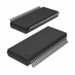 IDT74FCT16500ATPVG

The activity of extra discounts on wholesale prices is in full swing…
Please fill in your contact information and we will send you the latest wholesale price list.





