 ChipApex | Global Electronic Components Supplier
SEARCH
Search Product
Search Post
— IC芯片 | 连接器 | 传感器 | 被动器件 —
Search productSearch post
— IC芯片 | 连接器 | 传感器 | 被动器件 —
Consult the customer manager about the wholesale price.
consultation hotline:86-132-6715-2157
email:[email protected]
Contact the product manager for consultation. One-stop consultation is available.
Do you want a lower wholesale price? Please send us your inquiry and we will reply immediately.
The Infineon IJW120R100T1FKSA1 is a 1200 V CoolSiC™ Power Transistor utilizing a normally-on Silicon Carbide JFET technology in a PG-TO247-3 package. Key electrical parameters include a maximum drain-source on-state resistance (RDS(on)) of 100 mΩ at 25 °C and a typical total gate charge (QG) of 72 nC. The device supports a continuous drain current (IDS) of 26 A at 25 °C case temperature, with a pulsed current capability of 78 A. It features a maximum operating junction temperature (Tj) of 175 °C and a thermal resistance from junction to case (RthJC) of 0.78 K/W.
Verify the specific ordering suffix 'FKSA1' against official Infineon documentation to confirm packaging details and reel specifications. Ensure compatibility with the recommended direct drive technology using dedicated drivers like the 1EDI30J12Cx for optimal performance and safety.
Select this component for applications requiring high-frequency operation and reduced cooling requirements due to low intrinsic capacitance and fast switching. Note that as a normally-on device, it requires a negative gate voltage for turn-off and specific driver configurations to prevent unintended conduction during startup or fault conditions.
This part belongs to the CoolSiC™ family of active power switches based on silicon carbide. It combines the material properties of SiC with a JFET concept to achieve high performance and ruggedness. The device is designed to replace traditional silicon-based solutions in high-voltage power electronics to improve efficiency and compactness.
Direct replacement requires addressing the normally-on nature of the JFET. Cascode configurations with low-voltage MOSFETs or direct drive circuits are necessary alternatives to standard MOSFET drivers. Verify thermal management capabilities match the RthJC of 0.78 K/W.
The device turns off at negative gate voltage and turns on at zero volts. Designers must use a negative gate drive voltage for turn-off and can employ cascode configurations or direct drive technologies to ensure safe operation.
The datasheet specifies a maximum gate loop resistance for turn-off of 5.1 Ω. Using very low turn-off gate resistors, down to zero Ohms, is recommended to achieve maximum performance and avoid parasitic turn-on effects.
The monolithically integrated body diode exhibits switching performance close to external SiC Schottky barrier diodes with load-current-independent reverse recovery charge. Active turn-on of the channel is preferred for synchronous rectification to minimize losses.
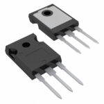 IJW120R100T1FKSA1
The activity of extra discounts on wholesale prices is in full swing…
Please fill in your contact information and we will send you the latest wholesale price list.





