ChipApex | Global Electronic Components Supplier
SEARCH
Search Product
Search Post
— IC芯片 | 连接器 | 传感器 | 被动器件 —
Search productSearch post
— IC芯片 | 连接器 | 传感器 | 被动器件 —
Consult the customer manager about the wholesale price.
consultation hotline:86-132-6715-2157
email:[email protected]
Contact the product manager for consultation. One-stop consultation is available.
Do you want a lower wholesale price? Please send us your inquiry and we will reply immediately.
The INA310B1QDGKRQ1 is an automotive-grade, ultra-precise current sense amplifier featuring a wide common-mode voltage range from –4 V to +110 V. It offers a fixed gain of 20 V/V with a signal bandwidth of 1.3 MHz and a slew rate of 2.5 V/µs. The device includes an integrated open-drain comparator with a 0.6 V internal reference and latching capability. Key electrical specifications include a maximum offset voltage of ±150 µV, a maximum gain error of 0.5%, and a typical CMRR of 140 dB. It operates on a single supply from 2.7 V to 20 V, drawing 1.6 mA of quiescent current.
Verify the specific suffix QDGKRQ1 corresponds to the VSSOP-8 package and reel packaging configuration. Confirm AEC-Q100 qualification status and functional safety documentation availability for your specific design requirements. Ensure the operating temperature range meets your environmental constraints.
Select this part for high-voltage sensing where precision and speed are critical. The B-version offers higher offset voltage tolerance compared to the A-version but maintains robust performance. Consider the 20 V/V gain for applications requiring moderate signal amplification. Evaluate the integrated comparator features to potentially reduce external component count in overcurrent protection designs.
This component belongs to the INA310x-Q1 family of ultra-precise current sense amplifiers designed for automotive environments. It shares architectural similarities with other high-voltage sense amplifiers but distinguishes itself through its zero-drift technology and integrated comparator functionality. The family supports multiple gain options to accommodate various dynamic range requirements in electric vehicle and industrial applications.
Official substitutes within the same family include INA310A1QDGKRQ1 for tighter offset specifications or variants with different gains such as INA310B2QDGKRQ1 (50 V/V), INA310B3QDGKRQ1 (100 V/V), INA310B4QDGKRQ1 (200 V/V), and INA310B5QDGKRQ1 (500 V/V). Verify pin compatibility and thermal characteristics when substituting.
When the RESET pin is left open or connected to GND, the comparator operates in transparent mode. When connected to the supply voltage, it enters latching mode, holding the output high after a trigger event until the RESET pin is pulled low or opened again.
The operational common-mode voltage range is –4 V to +110 V. However, the device can survive transient voltages up to +120 V and down to –20 V without permanent damage.
Yes, the device supports both unidirectional high-side and low-side current sensing configurations due to its wide common-mode input range that is independent of the supply voltage.
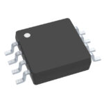 INA310B1QDGKRQ1
The activity of extra discounts on wholesale prices is in full swing…
Please fill in your contact information and we will send you the latest wholesale price list.