 ChipApex | Global Electronic Components Supplier

SEARCH
Search Product
Search Post
— IC芯片 | 连接器 | 传感器 | 被动器件 —
Search productSearch post
— IC芯片 | 连接器 | 传感器 | 被动器件 —
Consult the customer manager about the wholesale price.
consultation hotline:86-132-6715-2157
email:[email protected]
Contact the product manager for consultation. One-stop consultation is available.
Do you want a lower wholesale price? Please send us your inquiry and we will reply immediately.
IRF9910TRPBF-1 is listed in the FET, MOSFET Arrays range at ChipApex. The manufacturer field lists Infineon Technologies. Its product description is MOSFET 2N-CH 20V 10A 8SOIC. Review the specifications below when checking this part for your BOM.
The IRF9910TRPBF-1 is a dual N-channel HEXFET power MOSFET in an SO-8 package. Q1 (Control FET) has VDS of 20V, ID of 10A at 25°C, and RDS(on) max of 13.4mΩ at VGS=10V. Q2 (Synchronous FET) has ID of 12A at 25°C and RDS(on) max of 9.3mΩ at VGS=10V. Gate threshold voltage ranges from 1.65V to 2.55V. Thermal resistance RθJA is 62.5°C/W. Operating junction temperature reaches 150°C.
Verify the exact part number suffix against official manufacturer documentation to confirm tape and reel packaging specifications. Confirm that the component meets current RoHS compliance and halogen-free requirements as stated in the datasheet. Ensure the industrial qualification level aligns with your specific application reliability needs before finalizing procurement decisions.
Select this component when designing point-of-load converters requiring a dual N-channel MOSFET solution. The device offers distinct control and synchronous FET characteristics within a single SO-8 package. Consider the thermal resistance and current derating curves for proper heat dissipation planning in dense PCB layouts.
This component belongs to the HEXFET family of power MOSFETs manufactured by Infineon Technologies. It utilizes advanced planar technology to achieve low on-resistance and fast switching speeds. The dual configuration allows for compact design in synchronous buck converter topologies commonly used in digital electronics.
Check for direct pin-compatible alternatives with similar RDS(on) and voltage ratings. Verify thermal performance and gate charge parameters match your driver capabilities. Ensure any substitute maintains the same SO-8 package outline and moisture sensitivity level.
The maximum drain-to-source voltage (VDS) is 20V for both Q1 and Q2.
Q1 supports 10A while Q2 supports 12A at TA = 25°C with VGS @ 10V.
The gate threshold voltage (VGS(th)) ranges from 1.65V to 2.55V.
Explore related parts through FETs, MOSFETs, Transistors, Discrete Semiconductor Products, all product categories.
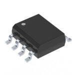 IRF9910TRPBF-1

The activity of extra discounts on wholesale prices is in full swing…
Please fill in your contact information and we will send you the latest wholesale price list.





