 ChipApex | Global Electronic Components Supplier

SEARCH
Search Product
Search Post
— IC芯片 | 连接器 | 传感器 | 被动器件 —
Search productSearch post
— IC芯片 | 连接器 | 传感器 | 被动器件 —
Consult the customer manager about the wholesale price.
consultation hotline:86-132-6715-2157
email:[email protected]
Contact the product manager for consultation. One-stop consultation is available.
Do you want a lower wholesale price? Please send us your inquiry and we will reply immediately.
ISPLSI 2128VE-100LT100 is listed in the Complex Programmable Logic Devices range at ChipApex. The manufacturer field lists Lattice Semiconductor Corporation. Its product description is IC CPLD 128MC 10NS 100TQFP. Review the specifications below when checking this part for your BOM.
The ispLSI 2128VE-100LT100 is a high-density, in-system programmable logic device from Lattice Semiconductor. It features 6000 PLD gates, 128 macrocells, and 28 I/O pins within a 100-pin LTQFP package. The device operates at a maximum frequency of 135 MHz with a propagation delay of 4 ns. It utilizes 3.3V E2CMOS technology for non-volatile reprogrammability via IEEE 1149.1 boundary scan. Key architectural elements include 32 Generic Logic Blocks (GLBs), three dedicated clock inputs, and eight dedicated input pins.
Verify component authenticity through authorized distributors or direct manufacturer channels. Confirm RoHS compliance status as lead-free options are available but may vary by production batch. Check for obsolescence notices or lifecycle changes prior to procurement planning.
Select this model for designs requiring 128 macrocells and 28 I/Os in a compact 100-pin surface mount package. Ensure voltage levels match the 3.0V to 3.6V operating range. Consider the -100 speed grade if timing constraints require a maximum frequency of 135 MHz.
This component belongs to the ispLSI 2128VE family, which offers 100% functional and pinout compatibility with the previous ispLSI 2128V series. It is designed to provide the ease of use of PLDs with the density of FPGAs, featuring enhanced pin locking and flexible global routing.
Direct functional replacements include other variants within the ispLSI 2128VE family with different speed grades or package types. Verify pin compatibility when substituting with older ispLSI 2128V models.
The maximum operating frequency (fmax) for the ispLSI 2128VE-100 is 135 MHz.
Yes, the outputs can be individually programmed as open-drain to support flexible bus interface capability and wired-OR logic.
The device features three dedicated clock input pins (Y0, Y1, Y2) that connect to all GLBs.
Explore related parts through Embedded, Integrated Circuits (ICs), all product categories, ChipApex homepage.
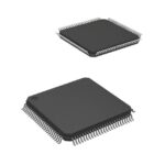 ISPLSI 2128VE-100LT100

The activity of extra discounts on wholesale prices is in full swing…
Please fill in your contact information and we will send you the latest wholesale price list.






