 ChipApex | Global Electronic Components Supplier

SEARCH
Search Product
Search Post
— IC芯片 | 连接器 | 传感器 | 被动器件 —
Search productSearch post
— IC芯片 | 连接器 | 传感器 | 被动器件 —
Consult the customer manager about the wholesale price.
consultation hotline:86-132-6715-2157
email:[email protected]
Contact the product manager for consultation. One-stop consultation is available.
Do you want a lower wholesale price? Please send us your inquiry and we will reply immediately.
The ispLSI 5512VE-80LF256I is a high-density, in-system programmable logic device from Lattice Semiconductor's ispLSI 5000VE family. It features 512 macrocells and 24,000 PLD gates within a 256-pin fpBGA package. Operating on a 3.3V supply with user-selectable 3.3V/2.5V I/O levels, the device supports up to 256 I/O pins. Key electrical specifications include a maximum operating frequency of 155 MHz and a propagation delay of 6.5 ns. The architecture utilizes SuperWIDE Generic Logic Blocks and a Global Routing Pool for efficient interconnect.
Verify that the specific ordering suffix LF256 corresponds to the 256-pin fine-pitch Ball Grid Array (fpBGA) package variant. Confirm the temperature grade 'I' indicates industrial range operation (-40°C to +85°C). Ensure programming equipment supports the IEEE 1149.1 JTAG interface required for in-system programming and boundary scan testing of this non-volatile device.
Select the ispLSI 5512VE over lower-density family members like the 5128VE or 5256VE when designs require more than 384 macrocells. Consider the -80 speed grade if timing analysis confirms that a 6.5 ns propagation delay meets the system requirements; faster grades may be available for stricter timing constraints. Evaluate power consumption estimates based on the number of active product terms and nets, as dynamic current scales with switching frequency.
The ispLSI 5512VE belongs to the second-generation SuperWIDE high-density PLD family. It serves as an evolution of earlier ispLSI 1000/2000/3000 architectures but offers enhanced pin-locking capabilities and a single-level global routing pool. Unlike the JEDEC-incompatible ispLSI 5000VA series, the VE family simplifies certain control logic to optimize performance and density for high-pin-count applications.
Direct pin-compatible replacements within the same package are limited due to architectural differences. The ispLSI 5512VA is not JEDEC compatible and may have different pinouts despite similar macrocell counts. Cross-family migration to FPGA solutions requires significant design restructuring. Verify that any substitute maintains the 256-pin fpBGA footprint and supports the required 3.3V/2.5V I/O voltage levels.
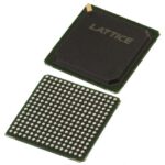 ISPLSI 5512VE-80LF256I

The activity of extra discounts on wholesale prices is in full swing…
Please fill in your contact information and we will send you the latest wholesale price list.





