ChipApex | Global Electronic Components Supplier
SEARCH
Search Product
Search Post
— IC芯片 | 连接器 | 传感器 | 被动器件 —
Search productSearch post
— IC芯片 | 连接器 | 传感器 | 被动器件 —
Consult the customer manager about the wholesale price.
consultation hotline:86-132-6715-2157
email:[email protected]
Contact the product manager for consultation. One-stop consultation is available.
Do you want a lower wholesale price? Please send us your inquiry and we will reply immediately.
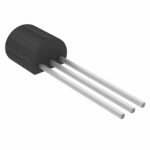
The J105 is an N-Channel Junction Field-Effect Transistor (JFET) designed for analog and digital switching applications requiring very low on-resistance. It is housed in a TO-92 3L bulk package. Key electrical characteristics include a Drain-Gate Voltage of 25 V, a Gate-Source Voltage of -25 V, and a maximum power dissipation of 625 mW at 25°C. The device features a Zero-Gate Voltage Drain Current (IDSS) of 500 mA and a Drain-Source On Resistance (RDS(on)) of 3.0 Ω. The Gate-Source Cut-Off Voltage ranges from -4.5 V to -10.0 V. Thermal resistance values are 125 °C/W junction-to-case and 357 °C/W junction-to-ambient.
Verify the specific ordering suffix against the official ON Semiconductor website, as Fairchild part numbers with underscores may have been updated to dashes following the company integration. Ensure the component source is an authorized distributor to guarantee authenticity and traceability, as counterfeit parts can compromise performance. Confirm that the package type matches the required TO-92 3L specification for your assembly process.
Select the J105 when a low RDS(on) of 3.0 Ω is required compared to the J106 or J107 variants. Consider the IDSS range of 500 mA and the VGS(off) limits of -4.5 V to -10.0 V to ensure compatibility with the control voltage levels in the target circuit. Evaluate the thermal constraints based on the 625 mW power dissipation rating and the specific ambient temperature conditions of the application environment.
The J105 belongs to a family of N-Channel Switches that includes the J106 and J107 models. These devices share similar packaging and basic structural characteristics but differ in their electrical thresholds and on-resistance values. The J105 represents the variant with the lowest on-resistance and highest drain current capability within this specific series, sourced from Process 59.
Direct substitutes within the same datasheet include the J106 and J107. The J106 offers 6.0 Ω RDS(on) and 200 mA IDSS, while the J107 provides 8.0 Ω RDS(on) and 100 mA IDSS. When replacing the J105 with these alternatives, verify that the higher on-resistance and lower current ratings do not exceed the design margins of the circuit.

The activity of extra discounts on wholesale prices is in full swing…
Please fill in your contact information and we will send you the latest wholesale price list.