 ChipApex | Global Electronic Components Supplier
SEARCH
Search Product
Search Post
— IC芯片 | 连接器 | 传感器 | 被动器件 —
Search productSearch post
— IC芯片 | 连接器 | 传感器 | 被动器件 —
Consult the customer manager about the wholesale price.
consultation hotline:86-132-6715-2157
email:[email protected]
Contact the product manager for consultation. One-stop consultation is available.
Do you want a lower wholesale price? Please send us your inquiry and we will reply immediately.
The onsemi J109 is a single N-channel Junction Field-Effect Transistor (JFET) designed for general-purpose switching and amplification applications. It utilizes silicon technology and is housed in a TO-92 through-hole package with three pins. The device supports a maximum drain-source current of 40 mA at 15 V and features a low on-resistance of 12 Ω. It operates within a junction temperature range of -55°C to 150°C, with a maximum power dissipation of 625 mW. The breakdown voltage is rated at 25 V, and the cutoff voltage is specified at 2 V when tested at 10 nA input current.
Verify the specific ordering suffix against official onsemi documentation to confirm exact electrical tolerances and testing criteria. Ensure the procurement channel provides genuine components with traceable manufacturing data. Cross-reference the part number with the latest datasheet revisions to confirm compliance with current specifications before finalizing purchase orders.
Select this component for designs requiring an N-channel JFET with moderate current handling capabilities. The TO-92 package is appropriate for prototyping or low-volume production where through-hole mounting is preferred. Consider the 625 mW power dissipation limit when designing heat management strategies for enclosed enclosures or high ambient temperature conditions.
The J109 belongs to the family of small-signal junction field-effect transistors manufactured by onsemi. These devices are engineered for reliability in discrete semiconductor applications. The TO-92 form factor represents a standard cylindrical plastic package widely used in consumer electronics and industrial instrumentation for low-power transistor functions.
Publicly confirmed substitute part numbers are not available in the provided source material. Engineers should consult official cross-reference guides or manufacturer compatibility lists to identify equivalent N-channel JFETs with matching pinouts and electrical ratings.
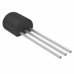 J109
J109
The activity of extra discounts on wholesale prices is in full swing…
Please fill in your contact information and we will send you the latest wholesale price list.





