 ChipApex | Global Electronic Components Supplier
SEARCH
Search Product
Search Post
— IC芯片 | 连接器 | 传感器 | 被动器件 —
Search productSearch post
— IC芯片 | 连接器 | 传感器 | 被动器件 —
Consult the customer manager about the wholesale price.
consultation hotline:86-132-6715-2157
email:[email protected]
Contact the product manager for consultation. One-stop consultation is available.
Do you want a lower wholesale price? Please send us your inquiry and we will reply immediately.
The onsemi J112 is an N-channel depletion mode Junction Field-Effect Transistor (JFET) designed for chopper applications. It operates within a drain-gate voltage range of -35 Vdc and a gate-source voltage limit of -35 Vdc. The device supports a maximum total power dissipation of 350 mW at 25°C ambient temperature, with a derating factor of 2.8 mW/°C above this threshold. Electrical characteristics include a zero-gate-voltage drain current (IDSS) ranging from 2.0 mA to 20 mA and a static drain-source on-resistance (rDS(on)) up to 50 Ω. The component functions reliably across an operating and storage junction temperature range of -65°C to +150°C.
Verify the specific ordering suffix against the manufacturer's documentation to confirm package style and environmental compliance. Standard bulk packages differ from tape and reel configurations. Confirm that the selected variant matches the required pinout style for the intended PCB layout. Ensure the procurement channel sources components directly from authorized distributors to maintain traceability and quality assurance standards.
Select the J112 when a low-noise, high-impedance N-channel switch is required for precision analog signal routing. Compare IDSS ranges and rDS(on) limits against circuit requirements to ensure adequate drive capability. Consider the TO-92 through-hole package constraints versus surface-mount alternatives like the MMBFJ112 if board space is limited. Validate thermal management needs based on the 350 mW dissipation rating in the final enclosure environment.
The J112 belongs to the J11x series of N-channel silicon field-effect transistors manufactured by onsemi. This family includes the J111 and J113 variants, which share similar structural designs but differ in electrical parameters such as IDSS and VGS(off). These devices are commonly utilized in instrumentation and measurement equipment where low offset voltages and high input impedance are critical for signal integrity.
Public confirmed substitute part numbers: J111, J113, MMBFJ112, SST112, IFN160BST3TR, IFN201AST3TR, IFN160CST3TR, IFN160BST3, MMBF4093.
Pin 1 is Drain, Pin 2 is Source, and Pin 3 is Gate.
The maximum gate-source breakdown voltage is -35 Vdc.
The J112 has a lower zero-gate-voltage drain current (IDSS) range of 2.0 mA to 20 mA compared to the J111, which typically exhibits higher current values.
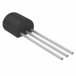 J112
J112
The activity of extra discounts on wholesale prices is in full swing…
Please fill in your contact information and we will send you the latest wholesale price list.






