 ChipApex | Global Electronic Components Supplier
SEARCH
Search Product
Search Post
— IC芯片 | 连接器 | 传感器 | 被动器件 —
Search productSearch post
— IC芯片 | 连接器 | 传感器 | 被动器件 —
Consult the customer manager about the wholesale price.
consultation hotline:86-132-6715-2157
email:[email protected]
Contact the product manager for consultation. One-stop consultation is available.
Do you want a lower wholesale price? Please send us your inquiry and we will reply immediately.
The JFE150DBVT is an N-channel JFET in a 5-pin SOT-23 package. It features ultra-low voltage noise of 0.8 nV/√Hz at 1 kHz with 5 mA drain current and 1.8 fA/√Hz current noise. The device offers high transconductance of 68 mS, low input capacitance of 24 pF, and maximum gate current of 10 pA. It withstands ±40 V breakdown voltages for gate-to-source/drain and drain-to-source terminals. Operating junction temperature ranges from -40°C to +125°C.
Verify the specific DBVT suffix corresponds to the 5-pin SOT-23 package configuration. Confirm RoHS compliance status and lead times directly with Texas Instruments or authorized distributors. Ensure design implementation accounts for the specified thermal resistance values and absolute maximum ratings to maintain device reliability during operation.
Select this component for applications requiring the lowest possible noise-to-power efficiency. The user-settable quiescent current allows optimization between power consumption and noise performance across a wide range. Consider the integrated clamp nodes if external protection components are undesirable due to leakage or non-linear capacitance concerns.
This discrete JFET utilizes Texas Instruments' modern analog bipolar process technology. It provides superior noise characteristics compared to older discrete JFET technologies. The device is designed to offer flexibility in biasing while maintaining excellent noise performance for currents ranging from 50 μA to 20 mA.
No public confirmed substitute part numbers are available in the documentation.
The device features integrated diodes connected to separate clamp nodes (VCH and VCL) that steer current from the gate during surges or ESD events, eliminating the need for external protection devices.
Noise performance depends on the drain-to-source bias current. Increasing the bias current increases transconductance, which decreases input-referred thermal noise, allowing designers to trade off current consumption for lower noise.
Yes, by shorting pin 2 (VCL) to pin 3 (Gate), the device can fit into a three-pin socket, though this disables the negative clamp diode protection and slightly increases input capacitance.
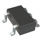 JFE150DBVT
The activity of extra discounts on wholesale prices is in full swing…
Please fill in your contact information and we will send you the latest wholesale price list.






