ChipApex | Global Electronic Components Supplier

SEARCH
Search Product
Search Post
— IC芯片 | 连接器 | 传感器 | 被动器件 —
Search productSearch post
— IC芯片 | 连接器 | 传感器 | 被动器件 —
Consult the customer manager about the wholesale price.
consultation hotline:86-132-6715-2157
email:[email protected]
Contact the product manager for consultation. One-stop consultation is available.
Do you want a lower wholesale price? Please send us your inquiry and we will reply immediately.
The LF353DR is a dual wideband JFET-input operational amplifier manufactured by Texas Instruments. It features a gain-bandwidth product of 3 MHz and a typical slew rate of 13 V/µs. The device operates on dual power supplies ranging from ±3.5 V to ±18 V, with a total supply voltage span between 7 V and 36 V. It draws a typical supply current of 3.6 mA per channel. Key electrical characteristics include a maximum input offset voltage of 5 mV, a typical input bias current of 50 pA, and a common-mode rejection ratio of 100 dB. The component is housed in an 8-pin SOIC package.
Verify the specific datasheet revision and manufacturing date code upon receipt to ensure compliance with RoHS3 standards. Confirm that the 8-SOIC package dimensions match the design footprint requirements. Check for any recent Product Change Notifications regarding assembly sites or material composition updates before finalizing the bill of materials.
Select this component when a dual-channel amplifier with JFET inputs is required for high-impedance signal paths. It is appropriate for designs needing moderate bandwidth and low noise without the complexity of bipolar inputs. Ensure the operating temperature range of 0°C to 70°C aligns with the system environment constraints.
This part belongs to the LF353 family of dual JFET-input operational amplifiers. It serves as a surface-mount variant of through-hole versions like the LF353N. The DR suffix indicates tape-and-reel packaging for automated assembly processes.
Direct pin-compatible alternatives within the same family include LF353D and LF353DG4. Verify functional equivalence if substituting with other dual JFET op-amps.
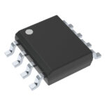 LF353DR

The activity of extra discounts on wholesale prices is in full swing…
Please fill in your contact information and we will send you the latest wholesale price list.