 ChipApex | Global Electronic Components Supplier

SEARCH
Search Product
Search Post
— IC芯片 | 连接器 | 传感器 | 被动器件 —
Search productSearch post
— IC芯片 | 连接器 | 传感器 | 被动器件 —
Consult the customer manager about the wholesale price.
consultation hotline:86-132-6715-2157
email:[email protected]
Contact the product manager for consultation. One-stop consultation is available.
Do you want a lower wholesale price? Please send us your inquiry and we will reply immediately.
LFE2-12SE-5F484I is listed in the Field Programmable Gate Array range at ChipApex. The manufacturer field lists Lattice Semiconductor Corporation. Its product description is IC FPGA 297 I/O 484FBGA. Review the specifications below when checking this part for your BOM.
The LFE2-12SE-5F484I is a Field Programmable Gate Array (FPGA) belonging to the LatticeECP2/M family, manufactured by Lattice Semiconductor Corporation. This device features 12,000 logic elements and supports up to 369 I/Os within a 484-pin FineLine BGA package. It operates with core voltages ranging from 1.14V to 1.26V and is rated for industrial temperature ranges of -40°C to +85°C. The architecture includes embedded block RAM totaling 2,151,424 bits and dedicated sysDSP™ blocks for high-performance multiply and accumulate operations. The component supports various source synchronous I/O standards and DDR memory interfaces.
Verify the specific suffix 'I' indicates the industrial temperature grade (-40°C to +85°C) rather than commercial grade. Confirm the package marking matches the 484-FPBGA specification. Ensure the ordering part number aligns with the ECP2M family datasheet DS1006 to avoid confusion with similar LFE2 variants that may have different pinouts or voltage requirements.
Select this model when system integration requires moderate logic density combined with extensive I/O capabilities. The presence of dedicated DDR support makes it suitable for applications interfacing with high-speed ADC/DAC devices. Consider the available sysDSP blocks if the design involves complex filtering or mathematical operations without external processors.
This component is part of the LatticeECP2/M family, which bridges the gap between low-density CPLDs and high-end FPGAs. The family is characterized by its non-volatile flash-based technology, allowing for instant-on functionality. The ECP2 series specifically targets cost-sensitive applications requiring high performance and low power consumption in compact form factors.
Direct replacements within the same family include other LFE2-12SE variants with different speed grades or package options, provided the pinout remains compatible. Cross-family migration to LatticeECP3 devices offers higher density but requires schematic and layout adjustments due to architectural differences.
Explore related parts through Embedded, Integrated Circuits (ICs), all product categories, ChipApex homepage.
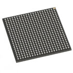 LFE2-12SE-5F484I

The activity of extra discounts on wholesale prices is in full swing…
Please fill in your contact information and we will send you the latest wholesale price list.





