 ChipApex | Global Electronic Components Supplier

SEARCH
Search Product
Search Post
— IC芯片 | 连接器 | 传感器 | 被动器件 —
Search productSearch post
— IC芯片 | 连接器 | 传感器 | 被动器件 —
Consult the customer manager about the wholesale price.
consultation hotline:86-132-6715-2157
email:[email protected]
Contact the product manager for consultation. One-stop consultation is available.
Do you want a lower wholesale price? Please send us your inquiry and we will reply immediately.
LFXP2-17E-5F484C is listed in the Field Programmable Gate Array range at ChipApex. The manufacturer field lists Lattice Semiconductor Corporation. Its product description is IC FPGA 358 I/O 484FBGA. Review the specifications below when checking this part for your BOM.
The LFXP2-17E-5F484C is a third-generation non-volatile FPGA from the LatticeXP2 family, utilizing FlexiFlash™ architecture for instant-on performance. It features 17 K logic cells (LUTs) and operates within a voltage range of 1.14V to 1.26V. The device includes up to 276 Kbits of embedded block RAM and 35 Kbits of distributed RAM. It supports DDR/DDR2 interfaces up to 400 Mbps and incorporates four analog PLLs for clock management. The component is housed in a 484-pin Fine Pitch Ball Grid Array (FPBGA) package with dimensions of 23x23 mm.
Verify the specific suffix '5' indicates the -5 speed grade corresponding to the required timing performance for your design. Confirm the 'E' designation aligns with the intended commercial temperature range specifications. Ensure the 484-FPBGA footprint matches your PCB layout constraints. Cross-reference the manufacturer's latest datasheet to confirm current production status and any potential package marking changes or alternate qualified test sites.
Select this model when system requirements demand non-volatile configuration without external PROMs. The 17 K LUT count suits moderate complexity logic designs. Verify that the available 276 Kbits of embedded memory meets buffering needs. Consider the four PLLs if multiple clock domains with precise phase shifting are necessary. Ensure the 484-pin package density fits within the physical space limitations of the target application enclosure.
This component belongs to the LatticeXP2 family, which bridges low-cost CPLDs and higher-density FPGAs. It targets high-volume applications needing small form factors and low power consumption. The series emphasizes reliability through its Flash-based architecture, distinguishing it from volatile SRAM-based counterparts that require external configuration memory chips.
Direct functional replacements within the same family include other LFXP2 variants such as LFXP2-5, LFXP2-8, LFXP2-30, or LFXP2-40, depending on logic resource requirements. Higher density alternatives may involve the LatticeECP2M series, though pinouts and feature sets differ significantly.
Explore related parts through Embedded, Integrated Circuits (ICs), all product categories, ChipApex homepage.


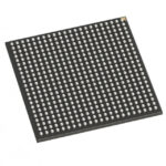 LFXP2-17E-5F484C

The activity of extra discounts on wholesale prices is in full swing…
Please fill in your contact information and we will send you the latest wholesale price list.



