 ChipApex | Global Electronic Components Supplier

SEARCH
Search Product
Search Post
— IC芯片 | 连接器 | 传感器 | 被动器件 —
Search productSearch post
— IC芯片 | 连接器 | 传感器 | 被动器件 —
Consult the customer manager about the wholesale price.
consultation hotline:86-132-6715-2157
email:[email protected]
Contact the product manager for consultation. One-stop consultation is available.
Do you want a lower wholesale price? Please send us your inquiry and we will reply immediately.
LMK1D2102LRGTT is listed in the Clock Buffers, Drivers range at ChipApex. The manufacturer field lists Texas Instruments. Its product description is LOW ADDITIVE JITTER LVDS BUFFER. Review the specifications below when checking this part for your BOM.
The LMK1D2102LRGTT is a low additive jitter LVDS clock buffer manufactured by Texas Instruments. It features five differential LVDS outputs and accepts universal input signals including LVDS, LVPECL, HCSL, CML, and LVCMOS. The device operates within a supply voltage range of 1.71 V to 3.465 V and supports maximum input frequencies up to 250 MHz. Key electrical parameters include a maximum propagation delay of 575 ps and a typical phase noise floor of -164 dBc/Hz at 156.25 MHz. It is housed in a 16-pin VQFN package and functions within an industrial temperature range of -40°C to +105°C.
Verify the specific suffix 'RGTT' corresponds to the 16-pin VQFN package and reel/cut-tape packaging configuration. Confirm RoHS compliance status through official manufacturer documentation prior to integration. Ensure design specifications align with the 1.71 V to 3.465 V operating voltage range and -40°C to +105°C temperature limits.
Select this component when low skew and ultra-low jitter are critical for distributing a single clock source to multiple LVDS loads. The dual-bank architecture allows independent control of output groups via enable pins. Consider the 575 ps maximum propagation delay and 20 ps maximum output skew for timing budget calculations in high-frequency designs.
The LMK1D2102LRGTT belongs to the LMK1D210xL family of dual-bank LVDS buffers. This series includes variants with different output counts, such as the LMK1D2104L (4-channel), LMK1D2106L (6-channel), and LMK1D2108L (8-channel). All members share similar low-jitter characteristics and universal input capabilities tailored for high-performance clock distribution networks.
Direct functional substitutes within the same family include the LMK1D2104L for higher channel density. Cross-family replacements like the CDCLVP2102 offer LVPECL outputs rather than LVDS. Verify pinout compatibility and output drive requirements when considering alternative Texas Instruments clock buffer models.
Explore related parts through Clock/Timing, Integrated Circuits (ICs), all product categories, ChipApex homepage.
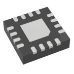 LMK1D2102LRGTT

The activity of extra discounts on wholesale prices is in full swing…
Please fill in your contact information and we will send you the latest wholesale price list.






