ChipApex | Global Electronic Components Supplier
SEARCH
Search Product
Search Post
— IC芯片 | 连接器 | 传感器 | 被动器件 —
Search productSearch post
— IC芯片 | 连接器 | 传感器 | 被动器件 —
Consult the customer manager about the wholesale price.
consultation hotline:86-132-6715-2157
email:[email protected]
Contact the product manager for consultation. One-stop consultation is available.
Do you want a lower wholesale price? Please send us your inquiry and we will reply immediately.
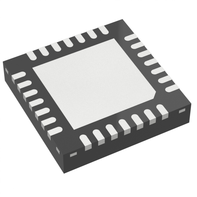
The LMKDB1202 is a low-power, high-compliance LP-HCSL clock multiplexer supporting PCIe Gen 1 through Gen 7. It features two differential inputs and two differential outputs within a 3mm x 3mm VQFN-20 package. The device provides extremely low additive jitter, with maximums of 5fs for PCIe Gen 5 and 3fs for PCIe Gen 6 at 156.25MHz. It supports both Common Clock (CC) and Independent Reference (IR) architectures, accepts input clocks with or without Spread Spectrum Clocking (SSC), and offers selectable 85Ω or 100Ω output impedance. Power supply options include 1.8V and 3.3V ±10%.
Verify the REY suffix corresponds to the 20-pin VQFN package. Confirm that the specific revision matches the SNAS927A datasheet dated April 2026. Ensure compatibility with required operating temperatures ranging from -40°C to 105°C ambient.
Select this model for designs requiring only two differential outputs. Compare against LMKDB1204 (4 outputs) or LMKDB1208 (8 outputs) if higher fan-out is needed. Verify that the 3mm x 3mm footprint fits the PCB layout constraints. Check if SMBus control is required, noting that the LMKDB1202 lacks dedicated SMBus pins compared to larger variants.
Part of the LMKDB family of ultra-low jitter clock muxes. Includes LMKDB1204 (REX package) and LMKDB1208 (RSL package). All devices share similar electrical characteristics and support PCIe Gen 1-7 standards.
LMKDB1204 (REX package) offers four outputs in a 4x4mm VQFN. LMKDB1208 (RSL package) provides eight outputs in a 6x6mm VQFN. Both maintain identical jitter performance and PCIe Gen 1-7 support.
 LMKDB1202REYR
The activity of extra discounts on wholesale prices is in full swing…
Please fill in your contact information and we will send you the latest wholesale price list.