 ChipApex | Global Electronic Components Supplier

SEARCH
Search Product
Search Post
— IC芯片 | 连接器 | 传感器 | 被动器件 —
Search productSearch post
— IC芯片 | 连接器 | 传感器 | 被动器件 —
Consult the customer manager about the wholesale price.
consultation hotline:86-132-6715-2157
email:[email protected]
Contact the product manager for consultation. One-stop consultation is available.
Do you want a lower wholesale price? Please send us your inquiry and we will reply immediately.
The LS7184N-S is a CMOS quadrature clock converter manufactured by LSI Computer Systems. It interfaces with incremental encoders to convert quadrature clocks into a single clock signal and an Up/Down direction control output. The device operates within a voltage range of +3V to +5.5V and features TTL and low voltage CMOS compatible I/Os. It supports x1, x2, and x4 resolution modes and includes programmable output pulse width capabilities ranging from 200ns to 140µs.
Verify the specific suffix 'S' indicates the SOIC package variant as documented in official LSI Computer Systems materials. Confirm that the LS7184N-S designation aligns with the manufacturer's current naming conventions for this quadrature converter. Ensure compatibility with system voltage requirements between +3V and +5.5V before procurement.
Select the LS7184N-S when a clock and direction output is required rather than separate up/down pulses provided by the LS7183. Consider the SOIC package format associated with the 'S' suffix for surface mount applications. Verify that the input interface matches standard optical or magnetic encoder outputs requiring conversion to digital logic levels.
The LS7184N-S belongs to the LS7183/LS7184 family of quadrature clock converters from LSI Computer Systems. While the LS7183 provides separate Up and Down clock outputs, the LS7184 variant specifically generates a combined clock and direction signal. This distinction allows designers to choose the output format that best suits their downstream counter or control logic architecture.
The LS7183 serves as a functional alternative if separate Up/Down clock outputs are preferred over a direction control signal. Both devices share similar electrical characteristics and encoder interface capabilities within the same product family.
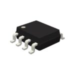 LS7184N-S

The activity of extra discounts on wholesale prices is in full swing…
Please fill in your contact information and we will send you the latest wholesale price list.





