ChipApex | Global Electronic Components Supplier
SEARCH
Search Product
Search Post
— IC芯片 | 连接器 | 传感器 | 被动器件 —
Search productSearch post
— IC芯片 | 连接器 | 传感器 | 被动器件 —
Consult the customer manager about the wholesale price.
consultation hotline:86-132-6715-2157
email:[email protected]
Contact the product manager for consultation. One-stop consultation is available.
Do you want a lower wholesale price? Please send us your inquiry and we will reply immediately.
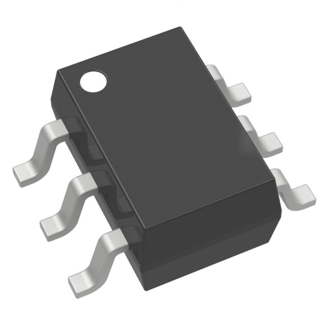
The LSK489 is a monolithic dual N-Channel JFET amplifier featuring industry-low input capacitance and low noise. It offers an input capacitance of 4pF and a noise voltage of 1.8nV/√Hz at 1kHz. The device provides high CMRR of 102dB and tight differential matching with VGS offset of 8mV typ. Available in SOT-23 6L, it supports continuous power dissipation of 300mW per side and operates within -55°C to +150°C junction temperature.
Verify the specific grade (A or B) required for your application, as IDSS ranges differ between grades. Confirm the SOT-23 6L package availability matches your PCB footprint requirements. Ensure operating conditions stay within the absolute maximum ratings for gate-source and drain-source voltages to maintain reliability.
Select the LSK489 when low input capacitance is critical to minimize intermodulation distortion compared to higher capacitance alternatives like the LSK389. Choose Grade A for tighter IDSS matching if precise current balancing is needed. Consider the SOT-23 package for surface mount designs requiring compact footprints while maintaining dual-JFET performance.
The LSK489 serves as a low-capacitance alternative to the LSK389, offering significantly lower gate-to-drain capacitance (4pF vs 25pF). While slightly noisier than the LSK389, its low capacitance enables simpler circuit designs. It shares pin compatibility with the LSK389 in TO-71 and SOIC packages, facilitating design upgrades.
The LSK389 is a compatible replacement in TO-71 and SOIC packages due to identical fit, form, and pinout. Note that the LSK389 has higher capacitance (25pF) but lower noise. For single-channel equivalents, refer to the LSK189 datasheet.
 LSK489 SOT-23 6L ROHS
The activity of extra discounts on wholesale prices is in full swing…
Please fill in your contact information and we will send you the latest wholesale price list.