ChipApex | Global Electronic Components Supplier
SEARCH
Search Product
Search Post
— IC芯片 | 连接器 | 传感器 | 被动器件 —
Search productSearch post
— IC芯片 | 连接器 | 传感器 | 被动器件 —
Consult the customer manager about the wholesale price.
consultation hotline:86-132-6715-2157
email:[email protected]
Contact the product manager for consultation. One-stop consultation is available.
Do you want a lower wholesale price? Please send us your inquiry and we will reply immediately.
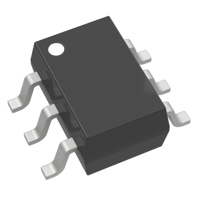
The LSK489A is a monolithic dual N-Channel JFET amplifier in a SOT-23 6L package. It features an input capacitance of 4pF and noise voltage of 1.8nV/√Hz at 1kHz. The device offers a common mode rejection ratio of 102dB, gate-to-source breakdown voltage of 60V, and drain saturation current ranging from 2.5mA to 8.5mA for the A grade. Maximum power dissipation is 300mW per side with a total of 500mW.
Verify the specific ordering suffix against official Linear Integrated Systems documentation to confirm exact electrical limits such as IDSS ranges or noise specifications. Ensure the component matches the required SOT-23 6L surface mount configuration. Confirm RoHS compliance status directly with the manufacturer or authorized distributors prior to procurement.
Select the LSK489A when extremely low input capacitance is critical to minimize intermodulation distortion in high-frequency circuits. Choose this part over higher capacitance alternatives like the LSK389 when circuit simplicity and lower production costs are prioritized alongside low-noise performance. Verify that the A-grade IDSS range meets the biasing requirements of the target application.
The LSK489 series represents a low-noise, low-capacitance monolithic dual N-Channel JFET amplifier. It is designed for precision instrumentation and sensor applications requiring tight offset voltage matching and low drift. The device combines interleaved JFET construction on a single silicon piece for excellent thermal tracking.
The LSK389 is pin-compatible and interchangeable in TO-71 and SOIC packages but has higher capacitance (25pF). No direct SOT-23 replacement is specified in the provided datasheet.
The typical common source input capacitance (CISS) is 4pF.
The LSK489 has significantly lower gate-to-drain capacitance (4pF) compared to the LSK389 (25pF).
The continuous power dissipation per side is 300mW at 25°C ambient temperature.
 LSK489A SOT-23 6L ROHS
The activity of extra discounts on wholesale prices is in full swing…
Please fill in your contact information and we will send you the latest wholesale price list.