ChipApex | Global Electronic Components Supplier

SEARCH
Search Product
Search Post
— IC芯片 | 连接器 | 传感器 | 被动器件 —
Search productSearch post
— IC芯片 | 连接器 | 传感器 | 被动器件 —
Consult the customer manager about the wholesale price.
consultation hotline:86-132-6715-2157
email:[email protected]
Contact the product manager for consultation. One-stop consultation is available.
Do you want a lower wholesale price? Please send us your inquiry and we will reply immediately.
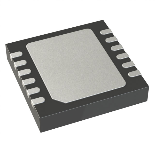
LT1469ACDF#TRPBF is listed in the Instrumentation, Op Amps, Buffer Amps range at ChipApex. The manufacturer field lists Analog Devices Inc.. Its product description is IC OPAMP GP 2 CIRCUIT 12DFN. Review the specifications below when checking this part for your BOM.
The LT1469ACDF#TRPBF is a dual precision high-speed operational amplifier featuring 16-bit accuracy. It offers a 90MHz gain bandwidth product and a 22V/µs slew rate, enabling fast settling times of 900ns for 10V steps. The device operates within a supply voltage range of ±5V to ±15V, with a maximum total supply voltage of 36V. Key electrical characteristics include a maximum input offset voltage of 125µV, low distortion of -96.5dB at 100kHz, and an input noise voltage density of 5nV/√Hz. It is housed in a space-saving 12-lead 4mm × 4mm plastic DFN package.
Verify the specific temperature grade and package variant against project requirements before ordering. Confirm that the tape and reel packaging aligns with automated assembly capabilities. Ensure compatibility with existing board layouts regarding the 12-lead DFN footprint and exposed pad thermal connection. Review absolute maximum ratings to prevent damage during operation or soldering processes.
Select this component when both high speed and high precision are critical simultaneously. The LT1469 is ideal for inverting applications due to its trimmed inverting input bias current. Consider the DF package for space-constrained designs requiring leadless mounting. Evaluate power supply constraints as performance specifications vary between ±5V and ±15V operating conditions.
The LT1469 series includes variants such as the LT1468 single-channel version and other package options like SOIC and PDIP. The AC suffix denotes a specific commercial temperature grade within the broader LT1469 family. This part represents a blend of Linear Technology's precision and speed technologies, targeting high-end data acquisition and signal processing markets.
Consult manufacturer documentation for officially confirmed substitute part numbers. Verify pinout compatibility and electrical parameter overlaps if considering alternative devices from different manufacturers.
The inverting input bias current is trimmed to zero at common mode voltage to minimize errors in inverting applications. In noninverting configurations, using balanced source resistance is not recommended as it degrades DC accuracy and increases noise.
The amplifier can drive up to 100pF in unity-gain and 300pF in a gain of -1. For larger capacitive loads, insert a small series resistor between the output and the load, and add a capacitor between the output and the inverting input to maintain stability.
The total input noise is optimized for a source resistance between 1kΩ and 20kΩ. Below 1kΩ, voltage noise dominates; above 20kΩ, input noise current becomes the dominant contributor. This optimization balances the internal noise sources for typical precision applications.
Explore related parts through Amplifiers, Linear, Integrated Circuits (ICs), all product categories.
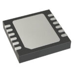 LT1469ACDF#TRPBF

The activity of extra discounts on wholesale prices is in full swing…
Please fill in your contact information and we will send you the latest wholesale price list.