ChipApex | Global Electronic Components Supplier

SEARCH
Search Product
Search Post
— IC芯片 | 连接器 | 传感器 | 被动器件 —
Search productSearch post
— IC芯片 | 连接器 | 传感器 | 被动器件 —
Consult the customer manager about the wholesale price.
consultation hotline:86-132-6715-2157
email:[email protected]
Contact the product manager for consultation. One-stop consultation is available.
Do you want a lower wholesale price? Please send us your inquiry and we will reply immediately.
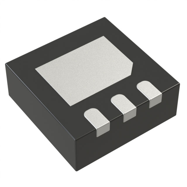
The LT6660KCDC-10#TRMPBF is a micropower series voltage reference from Analog Devices, featuring a fixed 10V output. It utilizes curvature compensation and laser-trimmed thin-film resistors to achieve high accuracy with a maximum initial tolerance of 0.5% and a maximum temperature coefficient of 50ppm/°C over the 0°C to 70°C specified range. The device operates within an input voltage range of VOUT + 0.9V to 20V, drawing a typical supply current of 270µA at this voltage setting. It provides up to 20mA of output current in a compact 3-lead 2mm × 2mm DFN package.
Verify the specific suffix #TRMPBF indicates tape and reel packaging with lead-free compliance. Confirm the KCDC designation corresponds to the 0.5% accuracy grade and 50ppm/°C temperature coefficient specifications. Ensure the operating environment remains within the 0°C to 70°C range for guaranteed performance parameters. Check for any obsolescence notices or limited availability status directly from the manufacturer before finalizing procurement plans.
Select this component when space constraints require a 2mm x 2mm DFN footprint while maintaining precision voltage referencing capabilities. The 10V output option is suitable for applications requiring higher reference levels without additional scaling circuitry. Consider the 0.5% initial accuracy and 50ppm/°C drift characteristics against system error budgets. Evaluate the 270µA supply current consumption for battery-powered designs where power efficiency is critical alongside accuracy requirements.
This part belongs to the LT6660 family of tiny micropower precision series references designed as space-saving alternatives to larger packages like the LT1460. The family offers various voltage options including 2.5V, 3V, 3.3V, 5V, and 10V with different accuracy grades (HC, JC, KC). The DC package denotes the 3-lead plastic DFN form factor with an exposed ground pad that must be soldered to the PCB for thermal and electrical connectivity.
LT1460ES6#PBF
No, the LT6660 family is designed to be stable with a large range of capacitive loads and does not require an output compensation capacitor, making it ideal for fast settling applications.
The device requires a minimum input-to-output voltage differential of 0.9V to maintain regulation, meaning the input voltage must be at least VOUT + 0.9V.
The device includes reverse-battery protection which keeps the reference from conducting reverse current, allowing it to withstand negative input voltages up to -15V.
 LT6660KCDC-10#TRMPBF

The activity of extra discounts on wholesale prices is in full swing…
Please fill in your contact information and we will send you the latest wholesale price list.