 ChipApex | Global Electronic Components Supplier

SEARCH
Search Product
Search Post
— IC芯片 | 连接器 | 传感器 | 被动器件 —
Search productSearch post
— IC芯片 | 连接器 | 传感器 | 被动器件 —
Consult the customer manager about the wholesale price.
consultation hotline:86-132-6715-2157
email:[email protected]
Contact the product manager for consultation. One-stop consultation is available.
Do you want a lower wholesale price? Please send us your inquiry and we will reply immediately.
LTC2865HMSE#PBF is listed in the Drivers, Receivers, Transceivers range at ChipApex. The manufacturer field lists Analog Devices Inc.. Its product description is IC TRANSCEIVER FULL 1/1 12MSOPEP. Review the specifications below when checking this part for your BOM.
The LTC2865HMSE#PBF is a low-power, full-duplex RS485/RS422 transceiver manufactured by Analog Devices Inc. It operates on a 3V to 5.5V supply and features ±60V fault protection on data lines during all modes, including power-down. The device supports selectable data rates of 20Mbps or 250kbps via the SLO pin. It includes an independent 1.65V to 5.5V logic supply (VL) for flexible digital interfacing. The component provides ±15kV ESD protection on interface pins, an extended common mode range of ±25V, and guaranteed failsafe receiver operation. It is housed in a 12-lead MSOP package with an exposed pad.
Verify the specific temperature grade suffix against the required operating range. Confirm the package type matches the PCB footprint design. Ensure the logic supply requirements align with the system's digital voltage levels before finalizing procurement.
Select this model when full-duplex communication is required alongside high fault tolerance. The independent VL pin allows compatibility with lower voltage logic systems while maintaining robust RS485 signaling. Verify that the thermal performance of the MSOP package meets the application's dissipation needs.
This component belongs to the LTC2862/LTC2863/LTC2864/LTC2865 family of ruggedized transceivers. It shares pinout compatibility with legacy parts like the LT1785 and LT1791 but offers superior fault protection and noise immunity characteristics suitable for harsh industrial environments.
LT1785
The data rate is selected using the SLO pin. Driving SLO high enables the 20Mbps high-speed mode, while driving it low selects the 250kbps low EMI slew-limited mode.
The VL pin provides an independent logic supply input ranging from 1.65V to 5.5V. This allows the logic inputs and outputs to operate at different voltage levels than the primary VCC supply.
Yes, the LTC2865 guarantees failsafe receiver operation. If the differential input voltage is within the threshold region for more than approximately 3µs, the output is forced to a logic 1 state.
Explore related parts through Interface, Integrated Circuits (ICs), all product categories, ChipApex homepage.
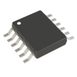 LTC2865HMSE#PBF

The activity of extra discounts on wholesale prices is in full swing…
Please fill in your contact information and we will send you the latest wholesale price list.





