 ChipApex | Global Electronic Components Supplier
SEARCH
Search Product
Search Post
— IC芯片 | 连接器 | 传感器 | 被动器件 —
Search productSearch post
— IC芯片 | 连接器 | 传感器 | 被动器件 —
Consult the customer manager about the wholesale price.
consultation hotline:86-132-6715-2157
email:[email protected]
Contact the product manager for consultation. One-stop consultation is available.
Do you want a lower wholesale price? Please send us your inquiry and we will reply immediately.
The LV5609LP-E is a vertical clock driver IC designed for CCD applications. It operates on a single supply voltage ranging from 2 V to 5.5 V and features CMOS input and output logic levels. The device contains one circuit with a fixed input-to-output ratio of 7:5. It is housed in a 24-VFQFN exposed pad package, specifically the 24-VCT (3.5x3.5) case outline. The component supports surface mount installation and functions within an operating temperature range of -20°C to +80°C.
Verify the specific package variant against the 24-VCT (3.5x3.5) specification during sourcing. Confirm that the operating temperature range of -20°C to +80°C meets the environmental requirements of the target assembly. Ensure compatibility with the 2 V to 5.5 V supply rail provided by the host system design.
Select this component when a dedicated vertical clock driver for CCD sensors is required. The 7:5 ratio is fixed; verify if this matches the sensor's timing requirements. The 24-VFQFN package requires appropriate PCB footprint design for the exposed pad thermal connection. Check if the -20°C lower temperature limit is sufficient for the intended deployment environment.
This part belongs to the Application Specific Clock/Timing category. It serves as a specialized interface between digital control logic and CCD imaging arrays. The CMOS I/O ensures compatibility with standard microcontroller or FPGA outputs commonly used in imaging systems.
No public substitute part numbers are confirmed in the available documentation.
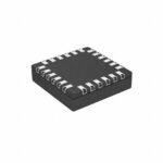 LV5609LP-E
The activity of extra discounts on wholesale prices is in full swing…
Please fill in your contact information and we will send you the latest wholesale price list.





