 ChipApex | Global Electronic Components Supplier
SEARCH
Search Product
Search Post
— IC芯片 | 连接器 | 传感器 | 被动器件 —
Search productSearch post
— IC芯片 | 连接器 | 传感器 | 被动器件 —
Consult the customer manager about the wholesale price.
consultation hotline:86-132-6715-2157
email:[email protected]
Contact the product manager for consultation. One-stop consultation is available.
Do you want a lower wholesale price? Please send us your inquiry and we will reply immediately.
The MA144769-287T is a surface mount low power step recovery diode manufactured by MACOM Technology Solutions. Designed for commercial wireless applications, it operates within an ambient temperature range of -65°C to +125°C. The device features a total capacitance of 0.8 pF to 1.2 pF at 1 MHz and 6 V reverse bias, with a maximum reverse voltage rating of 30 V at 10 µA. It supports nominal input frequencies from 0.1 GHz to 1.0 GHz, generating output frequencies up to 5 GHz. Key electrical parameters include a typical carrier lifetime of 20 ns, a maximum transition time of 50 ps, and a power dissipation limit of 250 mW.
Verify the specific ordering suffix against official documentation to confirm package style and packaging configuration. Confirm RoHS compliance status directly with the manufacturer or authorized distributor prior to procurement. Ensure that the selected component meets all absolute maximum ratings for reverse voltage and forward bias current required by the target application design.
Select this component for surface mount designs requiring low transition times and precise capacitance control. Evaluate the thermal constraints carefully, as the maximum body temperature during reflow soldering must not exceed +260°C. Consider the operating frequency range when determining suitability for specific multiplier orders, ensuring the input signal aligns with the specified 0.1 GHz to 1.0 GHz window.
This part belongs to MACOM's portfolio of surface mount low power step recovery diodes, which also includes the MAVR-044769-1279 variant. Both devices share identical electrical characteristics but differ in physical case styles, specifically SOT-23 and SC-79 configurations. They are engineered to address the size, power, and signal integrity requirements of modern wireless communication systems.
The MAVR-044769-1279 serves as a functional equivalent with identical electrical specifications but utilizes an SC-79 package instead of the SOT-23 form factor. Verify footprint compatibility and mounting pad dimensions before substituting. No other direct substitutes are documented in the provided datasheet.
The diode generates harmonics by storing charge during forward conduction. When the input signal reverses polarity, the charge is rapidly extracted, causing the device to snap to a higher impedance state and form a voltage pulse in the impulse circuit.
The absolute maximum reverse voltage is 30 V, and the maximum forward bias current is 50 mA. Exceeding these parameters may cause permanent damage to the device.
During permanent attachment via reflow soldering, the device body temperature must not exceed +260°C, while the tab temperature should not exceed +275°C.
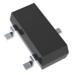 MA144769-287T
The activity of extra discounts on wholesale prices is in full swing…
Please fill in your contact information and we will send you the latest wholesale price list.





