 ChipApex | Global Electronic Components Supplier

SEARCH
Search Product
Search Post
— IC芯片 | 连接器 | 传感器 | 被动器件 —
Search productSearch post
— IC芯片 | 连接器 | 传感器 | 被动器件 —
Consult the customer manager about the wholesale price.
consultation hotline:86-132-6715-2157
email:[email protected]
Contact the product manager for consultation. One-stop consultation is available.
Do you want a lower wholesale price? Please send us your inquiry and we will reply immediately.
MAOC-009269-PKG003 is listed in the Clock Generators, PLLs, Frequency Synthesizers range at ChipApex. The manufacturer field lists MACOM Technology Solutions. Its product description is OSCILLATOR,VC,11.4-12.8 GHZ,5MMP. Review the specifications below when checking this part for your BOM.
The MAOC-009269 is an InGaP HBT-based voltage controlled oscillator (VCO) operating from 11.4 GHz to 12.8 GHz. It features a divide-by-two output at 5.7–6.4 GHz and an integrated buffer amplifier. The device requires no external matching components and operates on a +5V bias supply. Key electrical specifications include a typical phase noise of -83 dBc/Hz at a 10 kHz offset, tuning sensitivity of 0.22 GHz/V, and a tune voltage range of 1 V to 13 V. It is housed in a lead-free 5 mm x 5 mm x 0.9 mm 32-lead PQFN package.
Verify the specific ordering suffix when purchasing. The base part number MAOC-009269 is available in tape and reel configurations (e.g., TR0500 for 500 pieces or TR1000 for 1000 pieces). Sample boards (SMB003) are also listed. Confirm RoHS compliance and 260°C reflow compatibility requirements during procurement.
Select this component for applications requiring low phase noise and wide tuning ranges in the K/Ka-band spectrum. Ensure the design accommodates a +5V supply voltage and accounts for a total supply current of approximately 160 mA. The exposed pad must be connected to RF and DC ground to ensure proper thermal management and electrical performance.
This model belongs to the MACOM MAOC series of InGaP HBT voltage controlled oscillators. It shares architectural similarities with other models like the MAOC-009265 but targets higher frequency bands (11.4–12.8 GHz vs. 9.4–10.8 GHz). The family is characterized by integrated buffers and divide-by-two outputs for PLL integration.
Public confirmed substitute part numbers are not provided in the source material. Designers should consult MACOM directly for alternative solutions or cross-reference based on specific frequency and phase noise requirements.
Pin 12 provides the divided-by-two (RF/2) output signal, operating in the frequency range of 5.7 GHz to 6.4 GHz.
The exposed pad centered on the package bottom must be connected to RF and DC ground. Connecting all N/C pins to RF/DC ground in the layout is also recommended.
The absolute maximum supply voltage for both VCC and VBUFFER is +5.5 Vdc. Sustained operation near survivability limits is not recommended.
Explore related parts through Clock/Timing, Integrated Circuits (ICs), all product categories, ChipApex homepage.
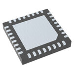 MAOC-009269-PKG003

The activity of extra discounts on wholesale prices is in full swing…
Please fill in your contact information and we will send you the latest wholesale price list.





