ChipApex | Global Electronic Components Supplier
SEARCH
Search Product
Search Post
— IC芯片 | 连接器 | 传感器 | 被动器件 —
Search productSearch post
— IC芯片 | 连接器 | 传感器 | 被动器件 —
Consult the customer manager about the wholesale price.
consultation hotline:86-132-6715-2157
email:[email protected]
Contact the product manager for consultation. One-stop consultation is available.
Do you want a lower wholesale price? Please send us your inquiry and we will reply immediately.
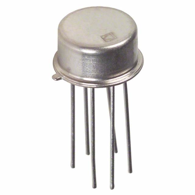
The MAT01AHZ is a matched monolithic dual NPN transistor manufactured by Analog Devices Inc. It utilizes an exclusive silicon nitride triple passivation process to ensure stability of critical parameters over temperature and time. The device features a typical offset voltage (VOS) of 40 µV with a maximum of 100 µV at 25°C, and a low temperature drift of 0.15 µV/°C. It offers high current gain (hFE) with a minimum of 500 at IC = 10 µA, extending up to 840 at IC = 10 mA. The component operates within a collector-emitter voltage range of 45 V and supports a continuous collector current of 25 mA. It is housed in a 6-pin metal header package (H-06) and functions reliably across a temperature range of -55°C to +125°C.
Verify the specific ordering suffix 'Z' indicates RoHS compliance when sourcing this component. Confirm the package option H-06 matches the required mechanical footprint for the design. Ensure that the absolute maximum ratings, particularly regarding reverse bias voltages on emitter-base junctions, are respected during circuit operation to prevent degradation of hFE matching characteristics.
Select the MAT01AHZ when ultra-low offset voltage and high current gain matching are critical requirements. This component is preferred over standard discrete transistors for applications demanding precise differential performance. Consider the thermal management capabilities if operating near the maximum power dissipation limits, as linearity may require derating at higher case temperatures.
The MAT01 series represents a family of matched monolithic dual transistors designed for high-precision analog applications. The AH variant specifically targets low offset voltage requirements compared to the GH variant. These devices are integral to maintaining accuracy in instrumentation systems where mismatch errors would otherwise degrade signal integrity.
Direct substitutes include other parts from the MAT01 family such as the MAT01GHZ for less stringent offset requirements. Verify pin compatibility and package dimensions before substituting with non-matched discrete transistor pairs, as electrical matching characteristics will differ significantly.
The maximum emitter-to-base voltage (BVEBO) is rated at 5 V. Applying reverse bias voltages exceeding this rating can result in the degradation of hFE and hFE matching characteristics.
Connecting the substrate (package) to a potential lower than either collector voltage can reduce collector-to-base (ICBO) and collector-to-emitter (ICES) leakage currents by a factor of 2 to 10 times.
The typical low-frequency noise voltage is 0.23 µV p-p measured from 0.1 Hz to 10 Hz.
 MAT01AHZ
The activity of extra discounts on wholesale prices is in full swing…
Please fill in your contact information and we will send you the latest wholesale price list.