 ChipApex | Global Electronic Components Supplier
SEARCH
Search Product
Search Post
— IC芯片 | 连接器 | 传感器 | 被动器件 —
Search productSearch post
— IC芯片 | 连接器 | 传感器 | 被动器件 —
Consult the customer manager about the wholesale price.
consultation hotline:86-132-6715-2157
email:[email protected]
Contact the product manager for consultation. One-stop consultation is available.
Do you want a lower wholesale price? Please send us your inquiry and we will reply immediately.
The MAX3173CAI is a triple driver/triple receiver multiprotocol transceiver designed for +3.3V single-supply operation. It supports V.28 (RS-232) and V.10/V.11 protocols, including RS-449, V.36, EIA-530, X.21, and RS-423. The device integrates an internal charge pump and low-dropout transmitter output stages to generate required voltage levels without external supplies. It features software-selectable DTE/DCE polarity inversion and includes short-circuit protection and thermal shutdown circuits. The component operates within a commercial temperature range of 0°C to +70°C and is housed in a 28-pin SSOP package.
Verify the specific suffix 'CAI' corresponds to the commercial temperature grade and SSOP package variant. Confirm RoHS compliance status as '+T' or '+' suffixes typically indicate lead-free versions, whereas non-suffixed parts may differ. Ensure the design accommodates the four surface-mount capacitors required for charge pump operation and power bypassing.
Select the MAX3173CAI when three control signal transceivers are required for multiprotocol communication. Choose this model over the MAX3171 if receiver input glitch filtering is not necessary for the application. Consider the MAX3172/MAX3174 variants if four control transceivers are needed instead of three.
This component belongs to the MAX317x family of +3.3V multiprotocol transceivers. It complements the MAX3170, which handles clock and data signals, to form complete DTE or DCE interface ports. The MAX3173 specifically omits the 10µs receiver input de-glitching feature found in the MAX3171, making it suitable for applications where such filtering is unnecessary.
The MAX3171CAI+ is a parameter-equivalent alternative that includes 10µs receiver input de-glitching. Direct substitutes include other MAX3173 variants with different packaging or suffixes, provided the electrical characteristics remain identical.
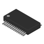 MAX3173CAI
The activity of extra discounts on wholesale prices is in full swing…
Please fill in your contact information and we will send you the latest wholesale price list.





