ChipApex | Global Electronic Components Supplier

SEARCH
Search Product
Search Post
— IC芯片 | 连接器 | 传感器 | 被动器件 —
Search productSearch post
— IC芯片 | 连接器 | 传感器 | 被动器件 —
Consult the customer manager about the wholesale price.
consultation hotline:86-132-6715-2157
email:[email protected]
Contact the product manager for consultation. One-stop consultation is available.
Do you want a lower wholesale price? Please send us your inquiry and we will reply immediately.
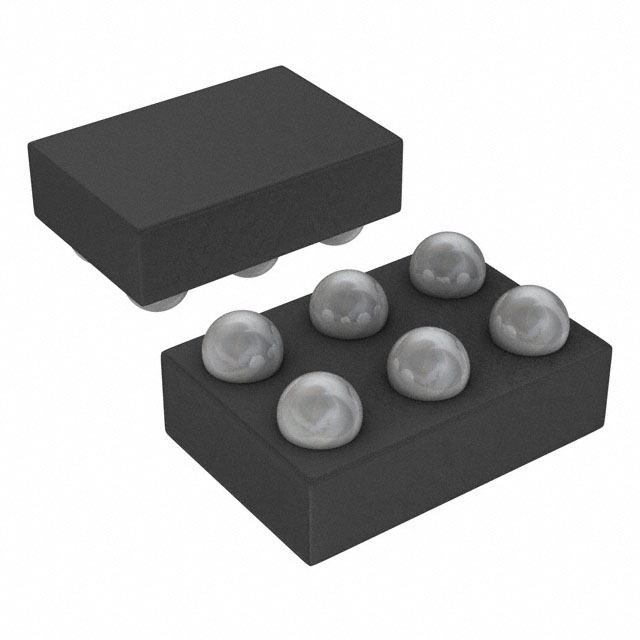
MAX44290ANT+ is listed in the Instrumentation, Op Amps, Buffer Amps range at ChipApex. The manufacturer field lists Analog Devices Inc./Maxim Integrated. Its product description is IC OPAMP GP 1 CIRCUIT 6WLP. Review the specifications below when checking this part for your BOM.
The MAX44290ANT+ is a single-channel operational amplifier in a 6-bump WLP package. It operates from a supply voltage of 1.8V to 5.5V, with support for 1.7V between 0°C and +70°C. Key electrical parameters include a gain-bandwidth product of 15MHz, a slew rate of 7 V/µs, and an input offset voltage of 50 µV maximum at +25°C. The quiescent current is 750 µA, reducing to under 1 µA in shutdown mode. Input bias current is 500 fA, and the input voltage noise density is 12.7 nV/√Hz.
Verify the component designation matches the specific ordering information provided in official documentation. Confirm the package type corresponds to the 6-bump wafer-level configuration. Ensure environmental compliance requirements align with lead-free specifications. Validate operating temperature ranges against application constraints before procurement.
Select this device for applications requiring low-voltage operation combined with precision signal conditioning. The low input bias current makes it suitable for interfacing with high-impedance sensors. Consider the compact package size for space-constrained portable designs. Evaluate the shutdown feature if power management during idle states is critical.
This component belongs to the MAX44290 series of low-power, high-speed operational amplifiers manufactured by Analog Devices. It is designed for portable and industrial equipment where power efficiency and signal integrity are paramount. The series supports various signal-processing functions including filtering and amplification.
Consult official manufacturer documentation for verified substitute part numbers. Cross-reference pin configurations and electrical characteristics carefully when considering alternatives.
It utilizes an optimized input stage with an ultra-quiet integrated charge pump that powers the PMOS differential pair, eliminating crossover distortion common in traditional CMOS architectures.
In shutdown mode, both inputs and outputs enter a high-impedance state, allowing multiple outputs to be multiplexed onto a single line without external buffers.
Explore related parts through Amplifiers, Linear, Integrated Circuits (ICs), all product categories.
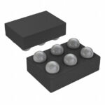 MAX44290ANT+

The activity of extra discounts on wholesale prices is in full swing…
Please fill in your contact information and we will send you the latest wholesale price list.