 ChipApex | Global Electronic Components Supplier

SEARCH
Search Product
Search Post
— IC芯片 | 连接器 | 传感器 | 被动器件 —
Search productSearch post
— IC芯片 | 连接器 | 传感器 | 被动器件 —
Consult the customer manager about the wholesale price.
consultation hotline:86-132-6715-2157
email:[email protected]
Contact the product manager for consultation. One-stop consultation is available.
Do you want a lower wholesale price? Please send us your inquiry and we will reply immediately.
MB88151APNF-G-200-JNERE1 is listed in the Clock Generators, PLLs, Frequency Synthesizers range at ChipApex. The manufacturer field lists Infineon Technologies. Its product description is IC FANOUT BUFFER 8SOP. Review the specifications below when checking this part for your BOM.
The MB88151APNF-G-200-JNERE1 is a Spread Spectrum Clock Generator designed for EMI reduction, manufactured by Infineon Technologies. It operates with a 3.3 V power supply and supports an input frequency range of 16.6 MHz to 33.4 MHz. As a multiply-by-2 variant, it generates an output frequency range of 33.2 MHz to 66.8 MHz. The device features cycle-cycle jitter of less than 100 ps-rms and a typical lock-up time of 25 ms. It consumes 5 mA at 24 MHz under no-load conditions and functions within an operating temperature range of -40 °C to +85 °C. The component is housed in an 8-pin SOP package.
Verify the specific suffix JNERE1 against the manufacturer's current ordering guide to confirm packaging type and reliability grade. Check for End-of-Life notifications or product change notices, as this component may have limited availability. Ensure compatibility with the required modulation rate pins SEL0 and SEL1 during procurement planning.
Select the CY88151A-200 variant when a frequency doubling function is required for inputs between 16.6 MHz and 33.4 MHz. Confirm that the system requires CMOS hysteresis inputs for control pins SEL0, SEL1, and ENS. Verify that the load capacitance on the CKOUT pin does not exceed 15 pF to maintain specified slew rate and duty cycle characteristics.
This component belongs to the CY88151A family of Spread Spectrum Clock Generators. It is functionally equivalent to the MB88151A series previously documented by Cypress Semiconductor before integration into Infineon's portfolio. The part number indicates a multiply-by-2 configuration with specific packaging and reliability grading.
Direct substitutes include other parts from the CY88151A family, such as the CY88151APNF-G-100-JNERE1 for multiply-by-1 applications. Cross-referencing with the MB88151A series is necessary for legacy designs. Ensure any replacement maintains the same SOP-8 package and 3.3 V operating voltage.
Modulation type is set using the SEL0 and SEL1 pins. Center spread is selected with LL (±1.5%) or LH (±0.5%), while down spread is selected with HL (-1.0%) or HH (-3.0%).
The cycle-cycle jitter is specified as less than 100 ps-rms for both the CY88151A-100 and CY88151A-200 variants under no-load conditions at 25 °C.
Unused input pins must not be left open; they should be connected to VDD or VSS using pull-up or pull-down resistors. Unused output pins should be left open.
Explore related parts through Clock/Timing, Integrated Circuits (ICs), all product categories, ChipApex homepage.
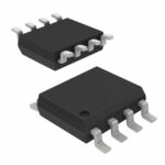 MB88151APNF-G-200-JNERE1

The activity of extra discounts on wholesale prices is in full swing…
Please fill in your contact information and we will send you the latest wholesale price list.






