 ChipApex | Global Electronic Components Supplier
SEARCH
Search Product
Search Post
— IC芯片 | 连接器 | 传感器 | 被动器件 —
Search productSearch post
— IC芯片 | 连接器 | 传感器 | 被动器件 —
Consult the customer manager about the wholesale price.
consultation hotline:86-132-6715-2157
email:[email protected]
Contact the product manager for consultation. One-stop consultation is available.
Do you want a lower wholesale price? Please send us your inquiry and we will reply immediately.
The MC100EP195FAR2G is a 3.3 V ECL Programmable Delay Chip (PDC) designed for clock deskewing and timing adjustment in high-speed systems. It provides variable delay of differential NECL/PECL input transitions with a digitally selectable resolution of approximately 10 ps. The device features a programmable range from 0 ns to 10 ns, with a total delay range spanning 2.2 ns to 12.2 ns due to fixed internal gate delays. It supports maximum input clock frequencies exceeding 1.2 GHz typical. Operating modes include PECL (VCC = 3.0 V to 3.6 V, VEE = 0 V) and NECL (VCC = 0 V, VEE = −3.0 V to −3.6 V). The component is housed in a 32-lead LQFP package.
Verify the ordering suffix 'R2G' corresponds to the specific tape and reel packaging configuration required for automated assembly processes. Confirm that the lead-free status aligns with environmental compliance standards applicable to the target manufacturing region. Ensure the LQFP-32 package dimensions match the PCB footprint design constraints before finalizing procurement orders.
Select this component when applications require sub-nanosecond resolution timing adjustments for differential ECL signals. Consider the cascading capability if the system demands a programmable range exceeding 10 ns. Evaluate power supply requirements carefully, as the device operates distinctly in either PECL or NECL configurations based on the VCC and VEE connections. Verify input voltage level compatibility with the selected mode using the VCF and VEF pins.
This part belongs to the MC100EP195 series of programmable delay chips manufactured by onsemi. It is specifically the tape and reel variant of the standard MC100EP195FAG. The series is characterized by temperature compensation and safety clamps on inputs. It serves as a critical timing element within the broader 100EP family of high-speed ECL logic components.
The MC100EP195FAR2G is a direct replacement for the discontinued MC100EP195FAR2. Both parts share identical electrical specifications and pinouts, differing only in the RoHS-compliant packaging suffix. No functional modifications are required when transitioning between these two specific part numbers.
The input threshold is controlled by the VCF and VEF pins. For LVCMOS, leave both open; for ECL, short them together; for LVTTL, connect a 1.5 V reference to VCF while leaving VEF open.
The D10 input controls the CASCADE and CASCADE outputs, enabling the chaining of multiple EP195 devices to increase the total programmable delay range.
Yes, due to the chain of multiplexers, the EP195 has a fixed minimum delay of approximately 2.2 ns, which is added to the programmable delay value.
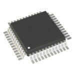 MC100EP195FAR2G
The activity of extra discounts on wholesale prices is in full swing…
Please fill in your contact information and we will send you the latest wholesale price list.






