 ChipApex | Global Electronic Components Supplier
SEARCH
Search Product
Search Post
— IC芯片 | 连接器 | 传感器 | 被动器件 —
Search productSearch post
— IC芯片 | 连接器 | 传感器 | 被动器件 —
Consult the customer manager about the wholesale price.
consultation hotline:86-132-6715-2157
email:[email protected]
Contact the product manager for consultation. One-stop consultation is available.
Do you want a lower wholesale price? Please send us your inquiry and we will reply immediately.
The MC100H642FNG is a clock driver and distribution IC designed for 68030/68040 microprocessors. It accepts ECL or TTL inputs and provides eight differential TTL outputs with a maximum frequency of 100 MHz. The device operates on a single +5.0 V supply (4.75V to 5.25V) within an operating temperature range of 0°C to 85°C. Packaged in a PLCC-28 surface-mount format, it includes internal divide-by-two and divide-by-four stages to generate required MPU clocks while maintaining strict part-to-part and within-part skew specifications.
Verify the component status as discontinued by checking official manufacturer records. Confirm that the PLCC-28 package dimensions match the target PCB footprint. Ensure the design supports the specific voltage levels and current requirements outlined in the datasheet before procurement.
Select this component when designing for 68030 or 68040 MPU architectures requiring precise clock synchronization. Verify compatibility between the chosen input source (TTL vs. PECL) and the system's existing clock generator. Ensure the application environment remains within the specified 0°C to 85°C operating temperature range.
This device belongs to the MC10H/100H642 series, which are specialized clock drivers. The '100' prefix indicates compatibility with 100K logic levels referenced to +5.0 V, distinguishing it from the standard MECL 10H compatible version. It serves as a critical interface for distributing synchronized clock signals to high-performance processors.
Public confirmed substitute part numbers are not available in the provided documentation. As the product is listed as discontinued, consult the manufacturer for potential obsolescence management options or alternative family members if direct pin-compatible replacements are required.
The SEL pin determines the active input source. A LOW signal selects the ECL input (DE/DE), while a HIGH signal selects the TTL input (DT).
The H642 uses internal differential PECL circuitry to achieve superior skew characteristics. To maintain a duty cycle of ±5% at 50 MHz, load capacitance and power supply variation must be limited according to the datasheet graphs.
A LOW signal on the Reset (R) pin forces all Q outputs LOW. The device also features a reset recovery time specification to ensure stable output states after the reset pulse ends.
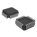 MC100H642FNG
The activity of extra discounts on wholesale prices is in full swing…
Please fill in your contact information and we will send you the latest wholesale price list.







