 ChipApex | Global Electronic Components Supplier

SEARCH
Search Product
Search Post
— IC芯片 | 连接器 | 传感器 | 被动器件 —
Search productSearch post
— IC芯片 | 连接器 | 传感器 | 被动器件 —
Consult the customer manager about the wholesale price.
consultation hotline:86-132-6715-2157
email:[email protected]
Contact the product manager for consultation. One-stop consultation is available.
Do you want a lower wholesale price? Please send us your inquiry and we will reply immediately.
MC100LVEL92DWR2G is listed in the Translators, Level Shifters range at ChipApex. The manufacturer field lists onsemi. Its product description is IC TRANSLATOR UNIDIR 20SOIC. Review the specifications below when checking this part for your BOM.
The MC100LVEL92DWR2G is a triple PECL input to LVPECL output translator manufactured by onsemi. It requires three power rails: VCC connected to the standard 5V PECL supply, LVCC connected to the 3.3V LVPECL supply, and Ground connected to the system ground plane. Both VCC and LVCC must be bypassed to ground with 0.01 µF capacitors. The device features 500 ps propagation delays and operates within an LVPECL voltage range of 3.0 V to 3.8 V and a PECL voltage range of 4.5 V to 5.5 V. It includes internal input pulldown resistors and meets JEDEC latchup test specifications.
Verify that the ordering suffix DWR2G corresponds to the SOIC-20 WB package in Tape & Reel format containing 1000 units per reel. Confirm RoHS compliance and Pb-Free status as specified in the datasheet. Ensure proper decoupling capacitors are included in the bill of materials for both VCC and LVCC pins to guarantee correct operation.
Select this component when interfacing circuits operating at 5V PECL levels with those requiring 3.3V LVPECL outputs. The device supports a wide operating temperature range from -40°C to +85°C. Consider the requirement for separate power rails and the availability of the PECL VBB pin for reference voltage generation or AC coupling rebiasing during system architecture planning.
This part belongs to the MC100LVEL92 series, which consists of triple translators designed for high-speed digital applications. The device utilizes a 20-pin Wide Body Small Outline Integrated Circuit (SOIC) package. It contains 247 transistors and is designed to meet strict reliability standards including UL 94 V-0 flammability ratings.
The MC100LVEL92DWG serves as a tube-packaged alternative to the DWR2G variant. Both share identical electrical characteristics and functionality but differ in shipping packaging configuration.
When the PECL VBB pin is not utilized for single-ended input switching references or AC coupled input rebiasing, it should be left open.
The Q output will default to LOW if the inputs are open or fall below GND + 1.3 V.
Explore related parts through Logic, Integrated Circuits (ICs), all product categories, ChipApex homepage.
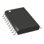 MC100LVEL92DWR2G

The activity of extra discounts on wholesale prices is in full swing…
Please fill in your contact information and we will send you the latest wholesale price list.





