 ChipApex | Global Electronic Components Supplier

SEARCH
Search Product
Search Post
— IC芯片 | 连接器 | 传感器 | 被动器件 —
Search productSearch post
— IC芯片 | 连接器 | 传感器 | 被动器件 —
Consult the customer manager about the wholesale price.
consultation hotline:86-132-6715-2157
email:[email protected]
Contact the product manager for consultation. One-stop consultation is available.
Do you want a lower wholesale price? Please send us your inquiry and we will reply immediately.
MC14504BDT is listed in the Translators, Level Shifters range at ChipApex. The manufacturer field lists onsemi. Its product description is IC TRANSLATOR UNIDIR 16TSSOP. Review the specifications below when checking this part for your BOM.
The MC14504BDT is a hex non-inverting level shifter utilizing CMOS technology, housed in a 16-pin TSSOP package. It facilitates signal translation between TTL and CMOS logic levels or between different CMOS voltage domains. The device operates with dual supply voltages (VCC and VDD) ranging from 3 to 18 Vdc. Key electrical parameters include a maximum propagation delay of 340 ns at 25°C with a 50 pF load, input current of ±0.1 µA, and output drive capabilities sufficient for low-power TTL loads.
Verify the specific suffix 'DT' corresponds to the TSSOP-16 package configuration required for your PCB layout. Confirm RoHS compliance status if environmental regulations apply to your manufacturing process. Ensure that the ordering documentation matches the exact part number to avoid discrepancies in package type or lead finish specifications.
Select this component when interfacing mixed-voltage logic families requiring unidirectional translation. The dual-supply architecture allows independent setting of input and output voltage thresholds. Verify that the application does not require bidirectional data flow, as this device supports only single-direction signal transfer.
This device belongs to the MC14504B series of hex level shifters manufactured by onsemi. It is designed to bridge communication gaps between different logic standards, specifically enabling TTL outputs to drive CMOS inputs or allowing CMOS-to-CMOS translation across varying supply rails without external components.
MC14504BDTG
Translation direction is determined by the relative values of the VCC and VDD supply pins. Setting VDD higher than VCC performs up-conversion, while setting VCC higher than VDD performs down-conversion.
The MODE pin selects the input logic threshold characteristics. Connecting it to VCC configures the device for TTL-compatible input levels, while connecting it to VSS configures it for standard CMOS input levels.
Explore related parts through Logic, Integrated Circuits (ICs), all product categories, ChipApex homepage.
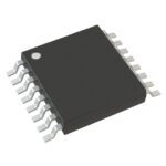 MC14504BDT

The activity of extra discounts on wholesale prices is in full swing…
Please fill in your contact information and we will send you the latest wholesale price list.





