ChipApex | Global Electronic Components Supplier

SEARCH
Search Product
Search Post
— IC芯片 | 连接器 | 传感器 | 被动器件 —
Search productSearch post
— IC芯片 | 连接器 | 传感器 | 被动器件 —
Consult the customer manager about the wholesale price.
consultation hotline:86-132-6715-2157
email:[email protected]
Contact the product manager for consultation. One-stop consultation is available.
Do you want a lower wholesale price? Please send us your inquiry and we will reply immediately.
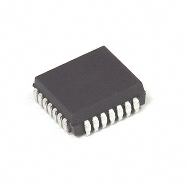
MC88915TFN70 is listed in the Clock Generators, PLLs, Frequency Synthesizers range at ChipApex. The manufacturer field lists NXP USA Inc.. Its product description is IC CLOCK DRIVER 28PLCC. Review the specifications below when checking this part for your BOM.
The MC88915TFN70 is a low skew CMOS PLL clock driver manufactured by NXP USA Inc. (formerly Motorola). It operates at a maximum frequency of 70 MHz for the 2X_Q output and 35 MHz for Q outputs, with a supply voltage range of 4.75V to 5.25V. The device features five phase-locked outputs (Q0–Q4) with less than 500 ps skew, plus inverted (Q5), doubled (2X_Q), and divided (Q/2) variants. Inputs are TTL-compatible, while outputs drive ±36 mA CMOS/TTL loads. Packaged in a 28-lead PLCC, it supports synchronous distribution for high-performance systems.
Verify component status as this part number may be discontinued or superseded. Confirm that the 70MHz variant meets specific thermal requirements, as the TFN70 version operates within a 0°C to +70°C temperature range, unlike other versions in the family which support -40°C to +85°C. Ensure compatibility with existing 5V power rails.
Select the MC88915TFN70 when a maximum operating frequency of 70 MHz on the 2X_Q output is required. Compare against TFN55 (55 MHz max) or TFN100 (100 MHz max) if frequency needs differ. Note that the TFN70 has a restricted commercial temperature range (0°C to +70°C) compared to industrial versions (-40°C to +85°C). Verify feedback configuration requirements for desired input-to-output frequency ratios.
This component belongs to the MC88915T family of low skew CMOS PLL clock drivers, which includes variants rated for 55, 70, 100, 133, and 160 MHz. The 'FN' suffix indicates a plastic PLCC package (Case 776-02). The device was originally produced by Motorola before being acquired by NXP.
Public confirmed substitute part numbers are not available in the provided documentation. Consider checking for newer iterations within the MC88915T family or consulting manufacturer obsolescence notices for direct replacements.
For the MC88915TFN70, the maximum operating frequency for the Q0–Q4 and Q5 outputs is 35 MHz, while the 2X_Q output can reach up to 70 MHz.
The FREQ_SEL pin provides a programmable divide-by option in the PLL feedback path. Holding it high selects divide-by-1, while holding it low selects divide-by-2, allowing the VCO to run in its optimal range (>20 MHz) even with lower frequency reference inputs.
The LOCK indicator output goes high when the loop achieves steady-state phase and frequency lock. It goes low if phase-lock is lost or if the PLL_EN pin is pulled low.
Explore related parts through Clock/Timing, Integrated Circuits (ICs), all product categories, ChipApex homepage.
 MC88915TFN70

The activity of extra discounts on wholesale prices is in full swing…
Please fill in your contact information and we will send you the latest wholesale price list.