 ChipApex | Global Electronic Components Supplier

SEARCH
Search Product
Search Post
— IC芯片 | 连接器 | 传感器 | 被动器件 —
Search productSearch post
— IC芯片 | 连接器 | 传感器 | 被动器件 —
Consult the customer manager about the wholesale price.
consultation hotline:86-132-6715-2157
email:[email protected]
Contact the product manager for consultation. One-stop consultation is available.
Do you want a lower wholesale price? Please send us your inquiry and we will reply immediately.
MCZ33905CS3EKR2 is listed in the Specialized range at ChipApex. The manufacturer field lists NXP USA Inc.. Its product description is IC INTERFACE SPECIALIZED 32SOIC. Review the specifications below when checking this part for your BOM.
The MCZ33905CS3EKR2 is a System Basis Chip (SBC) from the second-generation MC33905 family, designed for automotive body and safety applications. It integrates an enhanced high-speed CAN interface compliant with ISO11898-2 and -5 standards, alongside a single LIN 2.1/J2602-2 interface. The device provides a configurable MCU voltage regulator (VDD) available in 3.3 V or 5.0 V options, delivering up to 150 mA internally, extendable to 300 mA with an external ballast transistor. It features low power modes with quiescent currents as low as 15 µA, multiple wake-up sources, and advanced fail-safe state machine management.
Verify the specific ordering suffix against the manufacturer's official datasheet to confirm pinout compatibility and electrical characteristics. Ensure the selected variant matches the required VDD output voltage and LIN interface configuration for the target application design.
Select this component when a system requires integrated high-speed CAN and single LIN communication within a compact package. Consider the internal current limits of the VDD regulator and determine if an external ballast transistor is necessary to meet peak load requirements exceeding 150 mA.
This part belongs to the MC33905 family of System Basis Chips, which are optimized as companion chips for microcontrollers in automotive environments. The family offers scalability through various configurations of LIN interfaces and I/O pins, allowing designers to reuse hardware designs across different product tiers.
Compatible alternatives within the same family include MCZ33905CD3EK/R2 and MCZ33905BD5EK/R2. Verify that any substitute maintains the required SOIC-32 package and matches the specific VDD voltage and LIN interface count needed for the circuit.
The device operates within a supply voltage range of 5.5 V to 28 V, with a maximum input voltage capability of 27 VDC and support for 40 V load dump conditions.
The internal LDO provides up to 150 mA. To achieve higher current capabilities up to 300 mA, an optional external PNP ballast transistor can be implemented.
Yes, it includes an innovative fail-safe state machine linked to the SAFE pin, secured SPI with watchdog capabilities, and advanced cranking pulse management to ensure system reliability.
Explore related parts through Interface, Integrated Circuits (ICs), all product categories, ChipApex homepage.
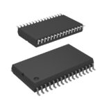 MCZ33905CS3EKR2

The activity of extra discounts on wholesale prices is in full swing…
Please fill in your contact information and we will send you the latest wholesale price list.





