ChipApex | Global Electronic Components Supplier
SEARCH
Search Product
Search Post
— IC芯片 | 连接器 | 传感器 | 被动器件 —
Search productSearch post
— IC芯片 | 连接器 | 传感器 | 被动器件 —
Consult the customer manager about the wholesale price.
consultation hotline:86-132-6715-2157
email:[email protected]
Contact the product manager for consultation. One-stop consultation is available.
Do you want a lower wholesale price? Please send us your inquiry and we will reply immediately.
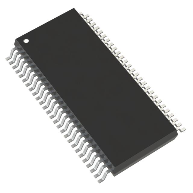
The MM908E626AVDWB is an integrated single-package solution combining a high-performance HC08 microcontroller with a SMARTMOS analog control IC. It features four low RDS(ON) half-bridge outputs, an embedded LIN physical layer, and a switchable 5.0 V voltage regulator (HVDD). The device operates within a supply voltage range of 8.0 V to 18 V and supports junction temperatures from -40 °C to 135 °C. Key specifications include a typical half-bridge on-resistance of 425 mΩ at 25 °C and peak current capability of 5.0 A per half-bridge. It includes 16 KB of flash memory, 512 bytes of RAM, and a 10-bit ADC.
Verify the specific suffix 'AVDWB' against official NXP documentation to confirm package type and temperature range. Ensure compatibility with the 54-pin SOICW-EP package requirements. Check for any specific ordering constraints or tape-and-reel options if applicable.
Select this component for applications requiring integrated MCU, motor drive, and LIN communication in a single package. Ensure the load current does not exceed the 5.0 A peak rating per half-bridge. Verify that the operating voltage stays within the 8.0 V to 18 V nominal range for optimal performance.
The MM908E626 belongs to the Freescale/NXP 908E series of integrated smart power devices. It is designed as a system-level solution for automotive body electronics, replacing discrete MCU, driver, and transceiver components to reduce PCB area and complexity.
Check for direct pin-to-pin replacements such as other variants in the 908E family (e.g., MM908E622, MM908E624, MM908E625) depending on specific feature requirements like high-side switches or different I/O counts. Confirm software compatibility if migrating between similar MCU cores.
 MM908E626AVDWB
The activity of extra discounts on wholesale prices is in full swing…
Please fill in your contact information and we will send you the latest wholesale price list.