 ChipApex | Global Electronic Components Supplier
SEARCH
Search Product
Search Post
— IC芯片 | 连接器 | 传感器 | 被动器件 —
Search productSearch post
— IC芯片 | 连接器 | 传感器 | 被动器件 —
Consult the customer manager about the wholesale price.
consultation hotline:86-132-6715-2157
email:[email protected]
Contact the product manager for consultation. One-stop consultation is available.
Do you want a lower wholesale price? Please send us your inquiry and we will reply immediately.
The MMBF4393LT1G is an N-channel Junction Field-Effect Transistor (JFET) manufactured by onsemi. It features a Drain-Source Voltage (VDS) of 30 Vdc and a Gate-Source Breakdown Voltage (V(BR)GSS) of 30 Vdc. The Zero-Gate-Voltage Drain Current (IDSS) ranges from 5.0 mAdc to 30 mAdc at VDS = 15 Vdc. Static Drain-Source On-Resistance (rDS(on)) is specified at 100 Ohms for ID = 1.0 mAdc. Input Capacitance (Ciss) is 14 pF at VDS = 0 Vdc and VGS = -15 Vdc. The device operates within a junction temperature range of -55°C to +150°C.
Verify the complete part number including the 'G' suffix to ensure Pb-Free compliance. Confirm the specific marking code 'M6G' matches the physical component received. Check the datasheet revision history for any updates to electrical characteristics or thermal ratings before finalizing design specifications.
Select this component when a low leakage current and defined on-resistance are required for signal path control. The MMBF4393L variant offers a lower IDSS range compared to the MMBF4391L and MMBF4392L counterparts. Ensure the driving circuit can handle the necessary gate-source voltage swing to fully deplete the channel for optimal isolation.
This device belongs to the MMBF439xL family of N-channel JFETs. It shares the same SOT-23 (TO-236) mechanical outline and maximum voltage ratings as the MMBF4391L and MMBF4392L. The primary distinction lies in the zero-gate-voltage drain current (IDSS) and corresponding gate-source cutoff voltage (VGS(off)), which define the specific switching thresholds for each model.
MMBF4393LT3G
Pin 1 is the Drain, Pin 2 is the Source, and Pin 3 is the Gate.
The MMBF4393L has the lowest IDSS range (5.0 to 30 mA) among the MMBF4391L, MMBF4392L, and MMBF4393L devices.
Yes, it exhibits low input capacitance (14 pF) and reverse transfer capacitance (3.5 pF), supporting fast switching times as detailed in the typical characteristics graphs.
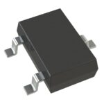 MMBF4393LT1G
The activity of extra discounts on wholesale prices is in full swing…
Please fill in your contact information and we will send you the latest wholesale price list.





