 ChipApex | Global Electronic Components Supplier
SEARCH
Search Product
Search Post
— IC芯片 | 连接器 | 传感器 | 被动器件 —
Search productSearch post
— IC芯片 | 连接器 | 传感器 | 被动器件 —
Consult the customer manager about the wholesale price.
consultation hotline:86-132-6715-2157
email:[email protected]
Contact the product manager for consultation. One-stop consultation is available.
Do you want a lower wholesale price? Please send us your inquiry and we will reply immediately.
The MMBF5457 is an N-channel Junction Field-Effect Transistor (JFET) manufactured by onsemi, housed in a SOT-23-3 surface-mount package. It serves as a low-level audio amplifier and switching transistor sourced from Process 55. Key electrical characteristics include a Gate-Source Breakdown Voltage of 25 V, a Zero-Gate Voltage Drain Current ranging from 1.0 to 5.0 mA at 15 V, and a maximum total device dissipation of 350 mW. The component operates within a junction temperature range of -55°C to +150°C.
Verify the specific ordering suffix against the manufacturer's current documentation to ensure correct packaging and marking configurations. Confirm RoHS compliance status and material declarations via official datasheets before integration. Cross-reference part numbers with authorized distributors to validate authenticity and traceability. Ensure storage conditions adhere to moisture sensitivity level requirements to maintain device reliability during assembly.
Select the MMBF5457 when designing circuits requiring an N-channel JFET with a 25 V breakdown voltage and moderate drain current capabilities. Consider its SOT-23-3 package for compact surface-mount designs. Evaluate the zero-gate voltage drain current specifications to match the required biasing conditions for audio or switching tasks. Verify thermal management needs based on the 350 mW power dissipation limit in the target application environment.
The MMBF5457 belongs to the MMBF54 series of N-channel JFETs, which also includes the MMBF5458 and MMBF5459 variants. These devices share similar structural characteristics but differ primarily in their zero-gate voltage drain current ranges. The series is designed for general-purpose amplification and switching, offering a cost-effective solution for small-signal applications across various consumer and industrial electronics.
The MMBF5458 and MMBF5459 are direct functional equivalents within the same family, differing mainly in drain current specifications. Verify that the alternative device's Idss range aligns with the circuit's biasing requirements. Ensure pinout compatibility and package dimensions remain identical to avoid PCB redesign.
Yes, the datasheet explicitly states that the source and drain terminals are interchangeable, allowing for flexible circuit orientation.
The maximum Gate-Source Breakdown Voltage (V(BR)GSS) is 25 V, measured with a gate current of 10 µA and VDS = 0.
Yes, the device is described as suitable for both low-level audio amplification and analog switching applications due to its high input impedance and low leakage characteristics.
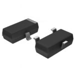 MMBF5457
The activity of extra discounts on wholesale prices is in full swing…
Please fill in your contact information and we will send you the latest wholesale price list.





