 ChipApex | Global Electronic Components Supplier
SEARCH
Search Product
Search Post
— IC芯片 | 连接器 | 传感器 | 被动器件 —
Search productSearch post
— IC芯片 | 连接器 | 传感器 | 被动器件 —
Consult the customer manager about the wholesale price.
consultation hotline:86-132-6715-2157
email:[email protected]
Contact the product manager for consultation. One-stop consultation is available.
Do you want a lower wholesale price? Please send us your inquiry and we will reply immediately.
The MMBFJ270 is a P-Channel Junction Field Effect Transistor (JFET) manufactured by onsemi. It features a maximum Drain-Gate Voltage of -30 V and a Gate-Source Breakdown Voltage of 30 V. The device operates within a junction temperature range of -55°C to 150°C with a total power dissipation of 225 mW. Electrical characteristics include a Zero-Gate Voltage Drain Current (IDSS) ranging from -2.0 mA to -15 mA at VDS = -15 V, and a Forward Transconductance (gfs) between 6000 µmhos and 15000 µmhos. The component is housed in an SOT-23 (TO-236) surface-mount package.
Verify the specific ordering suffix to confirm packaging format, such as Tape & Reel quantities. Confirm RoHS compliance status and ensure the component meets environmental standards required for the target assembly process. Cross-reference datasheet revision numbers to validate electrical parameters against current production batches.
Select this component based on its P-Channel configuration and voltage ratings suitable for low-voltage signal paths. Evaluate the transconductance and drain current specifications to ensure compatibility with the intended circuit impedance. Consider the thermal resistance and power dissipation limits relative to the PCB layout and ambient operating conditions.
This device belongs to the JFET category of discrete semiconductors produced by onsemi. It utilizes process 88 technology and is supplied in lead-free packages. The component is part of a broader portfolio of field-effect transistors designed for precision analog signal processing tasks requiring high input impedance and low noise characteristics.
MMBFJ270TR
The absolute maximum Drain-Gate Voltage is rated at -30 V.
It is specifically designed for low level analog switching, sample and hold circuits, and chopper stabilized amplifiers.
The device supports an operating and storage junction temperature range from -55°C to 150°C.
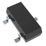 MMBFJ270
The activity of extra discounts on wholesale prices is in full swing…
Please fill in your contact information and we will send you the latest wholesale price list.





