 ChipApex | Global Electronic Components Supplier

SEARCH
Search Product
Search Post
— IC芯片 | 连接器 | 传感器 | 被动器件 —
Search productSearch post
— IC芯片 | 连接器 | 传感器 | 被动器件 —
Consult the customer manager about the wholesale price.
consultation hotline:86-132-6715-2157
email:[email protected]
Contact the product manager for consultation. One-stop consultation is available.
Do you want a lower wholesale price? Please send us your inquiry and we will reply immediately.
The MPC92433AE is a 1428 MHz dual-output LVPECL clock synthesizer manufactured by Integrated Device Technology, now part of Renesas Electronics. It operates on a 3.3 V supply and generates output frequencies from 42.50 MHz to 1428 MHz using an internal PLL with a VCO range of 1360–2856 MHz. The device features two differential LVPECL outputs (QA, QB) and supports frequency programming via a parallel interface or I²C bus. It includes an on-chip crystal oscillator for reference generation, synchronous clock stop functionality, and a LOCK indicator. The component is housed in a 48-lead LQFP package and functions within an ambient temperature range of –40°C to +85°C.
The MPC92433 has reached its end-of-life stage. The Last Time Buy deadline expired on January 31, 2014. No new production orders are accepted. Verification of availability is restricted to existing stock held by distributors or secondary market sources. Designers must initiate replacement strategies immediately due to the discontinuation status.
Select this component only if legacy compatibility with IDT clock architectures is required. Ensure the design accommodates the 48-lead LQFP package footprint. Verify that the system power supply provides a stable 3.3 V rail. Note that the AE suffix indicates lead-free, EPP, and RoHS compliance. Confirm that the target application can support the specific LVPECL termination requirements (50 Ω to VCC – 2.0 V).
This device belongs to the MPC9243x family of high-frequency clock synthesizers. It was originally produced by Integrated Device Technology (IDT) before IDT's acquisition by Renesas Electronics. The MPC92433 serves as a specialized solution for mid-to-high-performance telecom and computing markets, distinct from general-purpose microcontrollers or standard oscillators.
As the part is discontinued, direct substitutes should be sought from Renesas or other clock manufacturer portfolios. Potential replacements include modern LVPECL synthesizers with comparable frequency ranges and I²C configurability. Evaluate pin-compatible or functionally equivalent devices from current Renesas clock product lines.
The output frequency is configured using either a parallel hardware interface (via M, NA, NB, P pins) or a serial I²C interface. The parallel interface takes priority during startup, while I²C allows for dynamic changes and reading of configuration registers.
The device supports an on-chip crystal oscillator connected to XTAL1/XTAL2 pins for reference frequencies between 15 MHz and 20 MHz. Alternatively, an external LVCMOS compatible clock signal can be applied to the REF_CLK pin.
Yes. The frequency can be changed on the fly using the I²C interface. Specific commands such as INC (increment) and DEC (decrement) allow for rapid, small-step frequency adjustments suitable for frequency margining applications.
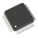 MPC92433AE

The activity of extra discounts on wholesale prices is in full swing…
Please fill in your contact information and we will send you the latest wholesale price list.





