 ChipApex | Global Electronic Components Supplier

SEARCH
Search Product
Search Post
— IC芯片 | 连接器 | 传感器 | 被动器件 —
Search productSearch post
— IC芯片 | 连接器 | 传感器 | 被动器件 —
Consult the customer manager about the wholesale price.
consultation hotline:86-132-6715-2157
email:[email protected]
Contact the product manager for consultation. One-stop consultation is available.
Do you want a lower wholesale price? Please send us your inquiry and we will reply immediately.
The MPC9315AC is a 2.5 V and 3.3 V CMOS PLL clock generator and driver designed for low-skew clock distribution in telecom, networking, and computing applications. It features eight LVCMOS outputs across three configurable banks (A, B, C) and two selectable reference inputs to support clock redundancy. The device supports output-to-input frequency ratios of 1:1, 2:1, 4:1, 1:2, and 1:4, with a maximum output skew of 120 ps. It operates within an ambient temperature range of -40°C to +85°C.
Verify the AC suffix indicates Pb-free packaging availability as specified in the datasheet. Confirm the FA suffix corresponds to standard leaded packages. Ensure the ordering code ending matches the required package variant. Check RoHS compliance status for specific manufacturing batches.
Select the MPC9315AC when zero-delay buffer configurations or spread spectrum clocking are required. Ensure the reference input frequency allows the internal VCO to operate between 75 MHz and 160 MHz for stable locking. Verify that the application requires LVCMOS compatible levels for both inputs and outputs.
The MPC9315AC belongs to the Advanced Clock Drivers Devices family from Freescale Semiconductor. It is specifically engineered to drive terminated transmission lines and minimize propagation delay. The device integrates a fully functional PLL without requiring external loop filter components.
Public confirmed substitute part numbers are not available in the provided documentation. Consult manufacturer resources for cross-reference information if alternative sourcing is necessary.
The device includes two selectable LVCMOS clock inputs (CLK0 and CLK1). The REF_SEL pin allows the user to select either input as the reference clock source.
VCCA provides power to the analog PLL circuitry. It requires an external RC filter to isolate sensitive analog circuits from digital switching noise on the main VCC supply.
Yes, by connecting an output to the selected feedback input (FB0 or FB1), the PLL aligns the output edge with the reference input edge, virtually eliminating propagation delay.
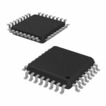 MPC9315AC

The activity of extra discounts on wholesale prices is in full swing…
Please fill in your contact information and we will send you the latest wholesale price list.





