 ChipApex | Global Electronic Components Supplier

SEARCH
Search Product
Search Post
— IC芯片 | 连接器 | 传感器 | 被动器件 —
Search productSearch post
— IC芯片 | 连接器 | 传感器 | 被动器件 —
Consult the customer manager about the wholesale price.
consultation hotline:86-132-6715-2157
email:[email protected]
Contact the product manager for consultation. One-stop consultation is available.
Do you want a lower wholesale price? Please send us your inquiry and we will reply immediately.
The MPC962308D-1 is a 3.3 V zero-delay buffer designed for high-speed clock distribution in PC, workstation, datacom, and telecom applications. It utilizes an internal PLL with an external feedback path to lock the output phase to the reference clock, achieving virtually zero propagation delay. The device provides eight LVCMOS outputs organized into two banks of four. Input-to-output skew is guaranteed at less than 250 ps, while output-to-output skew is under 200 ps. It supports clock frequencies from 10 MHz to 133 MHz and operates on a single 3.3 V supply within an ambient temperature range of –40 °C to +85°C.
Verify the specific suffix (e.g., D for SOIC or DT for TSSOP) and revision level against current manufacturer documentation. Confirm that the component meets the required industrial temperature range of –40 °C to +85°C for the intended application environment. Ensure compatibility with existing PCB footprints for the selected package type.
Select the MPC962308D-1 when a 1:8 ratio with identical frequency multiplication is required. Consider the -1H variant if faster rise and fall times are necessary for higher frequency integrity. Verify load capacitance requirements, as the maximum supported frequency decreases from 133 MHz to 100 MHz if the load exceeds 15 pF. Ensure the design accommodates the 3.3 V supply voltage constraints.
Originally manufactured by Motorola Semiconductor, this part was later managed by Freescale Semiconductor following corporate restructuring. The datasheet indicates it is functionally compatible with the Cypress CY2308 and CY23S08 devices. The MPC962308 series includes variants with different frequency division ratios, such as the -2, -3, -4, and -5H models, which offer 2X, 4X, or REF/2 outputs depending on the feedback configuration.
The datasheet explicitly states compatibility with the CY2308 and CY23S08. These devices may serve as direct pin-compatible replacements if their electrical specifications align with the system's jitter and skew requirements.
Zero delay is achieved by using an internal Phase-Locked Loop (PLL) combined with an external feedback path. This configuration locks the phase of the clock output to the reference clock phase, effectively eliminating propagation delay.
The device supports a clock I/O frequency range of 10 MHz to 133 MHz. However, the maximum frequency is dependent on the load capacitance; it is limited to 100 MHz if the load capacitance is 30 pF, and up to 133 MHz if the load is 15 pF or less.
Yes, the eight outputs are divided into two banks of four. Each bank can be tristated or driven based on the logic levels of the select inputs S1 and S2, allowing for flexible configuration and power-down states.
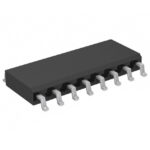 MPC962308D-1

The activity of extra discounts on wholesale prices is in full swing…
Please fill in your contact information and we will send you the latest wholesale price list.





