ChipApex | Global Electronic Components Supplier
SEARCH
Search Product
Search Post
— IC芯片 | 连接器 | 传感器 | 被动器件 —
Search productSearch post
— IC芯片 | 连接器 | 传感器 | 被动器件 —
Consult the customer manager about the wholesale price.
consultation hotline:86-132-6715-2157
email:[email protected]
Contact the product manager for consultation. One-stop consultation is available.
Do you want a lower wholesale price? Please send us your inquiry and we will reply immediately.
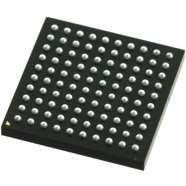
The MPC9850VM is a PLL-based clock generator designed for PowerQUICC III microprocessor applications. It features one circuit with LVCMOS, LVPECL, and crystal inputs, producing LVCMOS and LVDS outputs up to 500 MHz. The device operates on a 3.135V to 3.465V supply within a -40°C to +85°C range. Packaged in a 100-lead MAPBGA (11x11mm), it generates processor clocks and Rapid I/O signals using a 2 GHz VCO, supporting frequencies from 15.87 MHz to 200 MHz for banks A/B and 50/125/250/500 MHz for bank C.
Verify the VM suffix indicates a lead-free package variant of the standard MPC9850. Confirm availability as this component may be subject to end-of-life status given its 2005 datasheet revision and subsequent acquisition history. Ensure the 100-lead MAPBGA footprint matches the target PCB design constraints.
Select this device when designing for PowerQUICC III architectures requiring specific Rapid I/O clock rates. Ensure the input reference frequency matches the available 25 MHz or 33 MHz sources. Verify that the 3.3V core voltage and compatible LVCMOS/LVDS output drive levels align with the downstream logic requirements.
The MPC9850 was originally developed by Freescale Semiconductor for PowerQUICC III processors. The timing solutions organization was later acquired by Integrated Device Technology (IDT). The product line is now managed under Renesas Electronics Corporation following IDT's acquisition. This part represents a specialized clock generator for legacy high-performance communication processors.
No direct public substitute part numbers are documented in the provided source material.
 MPC9850VM
The activity of extra discounts on wholesale prices is in full swing…
Please fill in your contact information and we will send you the latest wholesale price list.