 ChipApex | Global Electronic Components Supplier
SEARCH
Search Product
Search Post
— IC芯片 | 连接器 | 传感器 | 被动器件 —
Search productSearch post
— IC芯片 | 连接器 | 传感器 | 被动器件 —
Consult the customer manager about the wholesale price.
consultation hotline:86-132-6715-2157
email:[email protected]
Contact the product manager for consultation. One-stop consultation is available.
Do you want a lower wholesale price? Please send us your inquiry and we will reply immediately.
The NA2100AFAE2D is a voltage-to-frequency converter manufactured by Nisshinbo Micro Devices Inc. using a CMOS process. It operates from a single supply of 3.0 V to 5.25 V and features an internal 2.5 V bandgap reference, with support for external references up to VDD. The full-scale output frequency is synchronized to the clock signal on the CLKIN pin, supporting frequencies from 32 kHz to 1 MHz. The nominal input range is 0 V to VREF. Key electrical characteristics include a maximum integral nonlinearity of ±0.018% of span and low consumption of approximately 3 mW (typical). It includes automatic power-down functionality when the clock input remains low.
Verify that the specific ordering suffix matches the required package type, version, packing direction, and quality grade. Confirm compliance with RoHS and halogen-free standards as indicated in the order information table. Ensure the selected variant aligns with the intended operating temperature range and application environment requirements specified in the datasheet.
Select this component for applications requiring a synchronous voltage-to-frequency conversion solution with low power consumption. Consider the buffer mode configuration based on the source impedance of the analog input signal. Evaluate the thermal resistance characteristics relative to the PCB layer count to ensure junction temperatures remain within safe operating limits during continuous operation.
This device belongs to the NA2100 series of voltage-to-frequency converters produced by Nisshinbo Micro Devices Inc. It is designed for general electronic equipment applications, including office equipment, telecommunications, and measuring instruments. The component utilizes a VSP-8-AF package and is manufactured using mature CMOS process technology.
No public confirmed substitute part numbers are documented in the official datasheet.
The device automatically enters a power-down mode when the CLKIN pin remains at a low level for approximately 1 ms, reducing the quiescent current significantly.
Yes, when operated in unbuffered mode (BUF = Low), the input circuit accepts analog inputs ranging from -0.15 V to VDD + 0.15 V.
The full-scale output frequency is set by the external system clock signal applied to the CLKIN pin, with the output varying between 10% and 90% of the clock frequency based on the input voltage.
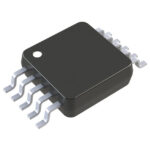 NA2100AFAE2D
The activity of extra discounts on wholesale prices is in full swing…
Please fill in your contact information and we will send you the latest wholesale price list.





