 ChipApex | Global Electronic Components Supplier

SEARCH
Search Product
Search Post
— IC芯片 | 连接器 | 传感器 | 被动器件 —
Search productSearch post
— IC芯片 | 连接器 | 传感器 | 被动器件 —
Consult the customer manager about the wholesale price.
consultation hotline:86-132-6715-2157
email:[email protected]
Contact the product manager for consultation. One-stop consultation is available.
Do you want a lower wholesale price? Please send us your inquiry and we will reply immediately.
The NB2305AC1DTG is a commercial-grade, 3.3 V zero delay clock buffer manufactured by onsemi. It accepts one reference input and drives five low-skew outputs using an internal Phase Locked Loop (PLL). The device operates within a frequency range of 15 MHz to 133 MHz and utilizes advanced 0.35 µm CMOS technology. Key electrical specifications include an output-to-output skew of less than 250 ps, device-to-device skew under 700 ps, and cycle-to-cycle jitter below 200 ps. The part is housed in an 8-pin TSSOP package with a supply voltage range of 3.0 V to 3.6 V.
Verify the specific suffix 'C1' confirms the commercial temperature range (0°C to 70°C) and 'DT' indicates the TSSOP-8 package. Confirm RoHS compliance status as the datasheet notes Pb-Free packages are available but requires checking the specific ordering code against current manufacturer lists for environmental declarations.
Select this component when a single-ended reference clock must be distributed to five loads with minimal skew. Ensure the load capacitance is matched across all outputs, including CLKOUT, to maintain zero input-output delay. For industrial environments (-40°C to 85°C), the 'I' suffix variant is required instead of the 'C' suffix used here.
This part belongs to the NB2305A family of 3.3 V zero delay buffers. The 'C1' designation identifies it as the base drive version operating in the commercial temperature range. Higher drive variants exist with the 'H' suffix (e.g., NB2305AC1HDG), which offer faster rise and fall times compared to the standard -1 devices.
Public confirmed substitute part numbers: None identified in verified source material.
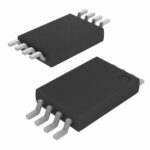 NB2305AC1DTG

The activity of extra discounts on wholesale prices is in full swing…
Please fill in your contact information and we will send you the latest wholesale price list.





