 ChipApex | Global Electronic Components Supplier

SEARCH
Search Product
Search Post
— IC芯片 | 连接器 | 传感器 | 被动器件 —
Search productSearch post
— IC芯片 | 连接器 | 传感器 | 被动器件 —
Consult the customer manager about the wholesale price.
consultation hotline:86-132-6715-2157
email:[email protected]
Contact the product manager for consultation. One-stop consultation is available.
Do you want a lower wholesale price? Please send us your inquiry and we will reply immediately.
NDD02N40T4G is listed in the Single FETs, MOSFETs range at ChipApex. The manufacturer field lists onsemi. Its product description is MOSFET N-CH 400V 1.7A DPAK. Review the specifications below when checking this part for your BOM.
The NDD02N40T4G is an N-channel power MOSFET from onsemi, rated for a drain-to-source voltage of 400 V and a continuous drain current of 1.7 A at 25°C case temperature. It features a maximum static drain-to-source on-resistance of 5.5 Ω at 10 V gate drive. The device is housed in a DPAK (CASE 369C) surface-mount package with a junction-to-case thermal resistance of 3.2 °C/W. Key electrical parameters include a gate threshold voltage of 0.8 to 1.6 V, total gate charge of 5.5 nC, and single-pulse avalanche energy capability of 120 mJ.
Verify the specific ordering suffix T4G corresponds to the DPAK tape and reel packaging configuration containing 2500 units per reel. Confirm that the component meets RoHS, Halogen-free, and BFR-free material requirements as specified in the datasheet documentation. Ensure compatibility with standard surface-mount assembly processes for the CASE 369C footprint.
Select this component for applications requiring 400 V blocking capability with moderate current handling up to 1.7 A. Consider the 5.5 Ω on-resistance for conduction loss calculations at 10 V gate drive. Evaluate the 3.2 °C/W junction-to-case thermal resistance against the expected power dissipation and heatsinking strategy to maintain safe operating temperatures within the -55 to +150 °C range.
This part belongs to the NDD02N40/NDT02N40 family of N-channel power MOSFETs manufactured by onsemi. The family includes variations such as the IPAK leaded version (NDD02N40-1G) and the SOT-223 surface-mount version (NDT02N40T1G). All variants share identical electrical characteristics but differ in physical package style and shipping configuration.
Direct substitutes within the same electrical specification and package include NDD02N40-1G (IPAK) and NDT02N40T1G (SOT-223), provided the mechanical form factor matches the design constraints. Cross-brand replacements must match the 400 V rating, 1.7 A current limit, and 5.5 Ω RDS(on) maximum.
The maximum single-pulse drain-to-source avalanche energy (EAS) is 120 mJ when tested at ID = 1 A.
The reverse recovery time (trr) is 146 ns under test conditions of VGS = 0 V, VDD = 30 V, IS = 1.7 A, and di/dt = 100 A/µs.
Explore related parts through FETs, MOSFETs, Transistors, Discrete Semiconductor Products, all product categories.
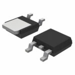 NDD02N40T4G

The activity of extra discounts on wholesale prices is in full swing…
Please fill in your contact information and we will send you the latest wholesale price list.





