 ChipApex | Global Electronic Components Supplier

SEARCH
Search Product
Search Post
— IC芯片 | 连接器 | 传感器 | 被动器件 —
Search productSearch post
— IC芯片 | 连接器 | 传感器 | 被动器件 —
Consult the customer manager about the wholesale price.
consultation hotline:86-132-6715-2157
email:[email protected]
Contact the product manager for consultation. One-stop consultation is available.
Do you want a lower wholesale price? Please send us your inquiry and we will reply immediately.
The NLV18VHC1GT08DFT2G is an automotive-grade CMOS logic gate featuring a single 2-input AND function. It operates within a supply voltage range of 4.5 V to 5.5 V and supports junction temperatures from -55°C to +125°C, with AEC-Q100 Grade 1 compliance for -40°C to +125°C. The device utilizes TTL-compatible input levels while maintaining CMOS output characteristics. Packaged in the SC-88A (SOT-353) format, it delivers symmetrical output impedance with 8 mA drive capability and typical propagation delays of 7 ns at 5.5 V.
Verify the specific ordering suffix matches the required tape and reel configuration. Confirm that the NLV prefix aligns with project requirements for unique site and control change protocols mandated by automotive quality standards. Ensure the component meets all applicable RoHS and halogen-free specifications before final integration into production assemblies.
Select this component when TTL input compatibility is necessary alongside high-speed CMOS performance. The device is suitable for applications demanding balanced propagation delays and low power dissipation. Verify that the operating voltage range strictly adheres to the 4.5 V minimum requirement specified for the GT series variants.
This part belongs to the NLV18VHC1Gxx and NLV18VHC1GTxx family of automotive logic gates manufactured by onsemi. The family encompasses various logic functions including NAND, NOR, buffers, and inverters. The GT suffix specifically denotes devices engineered with TTL-compatible input voltage levels, distinguishing them from the standard G series which utilize CMOS input thresholds.
NLV18VHC1G08DFT2G
The primary distinction lies in the input voltage levels; the GT variant features TTL-compatible inputs, whereas the standard G variant utilizes CMOS input voltage levels.
Yes, the device is AEC-Q100 qualified and PPAP capable, designed to operate reliably within the automotive temperature range of -40°C to +125°C.
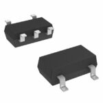 NLV18VHC1GT08DFT2G

The activity of extra discounts on wholesale prices is in full swing…
Please fill in your contact information and we will send you the latest wholesale price list.





