 ChipApex | Global Electronic Components Supplier

SEARCH
Search Product
Search Post
— IC芯片 | 连接器 | 传感器 | 被动器件 —
Search productSearch post
— IC芯片 | 连接器 | 传感器 | 被动器件 —
Consult the customer manager about the wholesale price.
consultation hotline:86-132-6715-2157
email:[email protected]
Contact the product manager for consultation. One-stop consultation is available.
Do you want a lower wholesale price? Please send us your inquiry and we will reply immediately.
The NLX2G04AMX1TCG is a dual inverter integrated circuit manufactured by onsemi, belonging to the NLX logic family. It operates within a supply voltage range of 1.65 V to 5.5 V and features two independent inverter circuits with two inputs each. The device utilizes a 6-ULLGA surface-mount package measuring 1x1 mm. Key electrical parameters include a maximum propagation delay of 7.5 ns at 5 V with 50 pF load, output currents of ±8 mA, and a static current of 1 µA. It supports an operating temperature range from -55 °C to +125 °C.
Verify component authenticity through authorized distributors or direct manufacturer channels. Confirm RoHS compliance status and check for product change notifications regarding packaging or material composition updates. Ensure storage conditions meet moisture sensitivity level requirements prior to assembly. Review datasheet revisions for any parameter adjustments affecting design integration.
Select this component when dual inverter functionality is required in a compact footprint. Consider the 1.65 V to 5.5 V operating range for compatibility with various logic families. Evaluate the 7.5 ns propagation delay against system timing constraints. Compare package dimensions and pinout against PCB layout specifications to ensure mechanical fit.
This part belongs to onsemi's NLX series of high-speed CMOS logic devices. The series focuses on providing robust performance in small packages suitable for portable and space-constrained applications. The dual inverter topology offers flexibility in digital circuit design, allowing for phase inversion or buffer implementation within minimal board area.
Check for cross-reference parts with identical logic function and package type. Verify voltage ranges and output drive capabilities match original specifications. Confirm thermal characteristics and operating temperature limits align with application requirements before substitution.
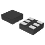 NLX2G04AMX1TCG

The activity of extra discounts on wholesale prices is in full swing…
Please fill in your contact information and we will send you the latest wholesale price list.





