 ChipApex | Global Electronic Components Supplier

SEARCH
Search Product
Search Post
— IC芯片 | 连接器 | 传感器 | 被动器件 —
Search productSearch post
— IC芯片 | 连接器 | 传感器 | 被动器件 —
Consult the customer manager about the wholesale price.
consultation hotline:86-132-6715-2157
email:[email protected]
Contact the product manager for consultation. One-stop consultation is available.
Do you want a lower wholesale price? Please send us your inquiry and we will reply immediately.
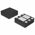
NTLJD4150PTBG is listed in the FET, MOSFET Arrays range at ChipApex. The manufacturer field lists onsemi. Its product description is MOSFET 2P-CH 30V 1.8A 6WDFN. Review the specifications below when checking this part for your BOM.
The NTLJD4150PTBG is a dual P-channel enhancement-mode MOSFET from onsemi, housed in a compact 6-lead WDFN package with dimensions of 2.2mm x 2.2mm and a height of 1mm. It features an exposed drain pad for efficient thermal dissipation. Key electrical specifications include a maximum drain-source voltage (Vds) of -30V and a continuous drain current (Id) of -3.4A at 25°C. The device exhibits a maximum on-resistance (Rds(on)) of 1Ω and a typical gate charge (Qg) of 2.2nC. It operates within a temperature range of -55°C to 150°C junction temperature, with a maximum power dissipation of 700mW.
Verify the specific ordering suffix against the manufacturer's official datasheet to ensure correct packaging and tape-and-reel specifications. Confirm that the component meets AEC-Q101 automotive qualification requirements if intended for automotive-grade deployments. Cross-reference the exact part number with the latest product release notes to validate availability and any potential design changes.
Select this component when space-constrained designs require dual P-channel switching capabilities. The low on-resistance supports efficient power handling in small form factors. Ensure the application voltage does not exceed the 30V rating and consider the thermal resistance of the PCB layout due to the exposed pad requirement for optimal performance.
This device belongs to onsemi’s uCool family of power MOSFETs, designed for high-efficiency power conversion. The dual configuration reduces board space compared to discrete solutions. It serves as a modern alternative to older SC-88 footprint components, offering improved thermal characteristics while maintaining compatibility with existing mechanical layouts.
NTLJD4150PT1G
Explore related parts through FETs, MOSFETs, Transistors, Discrete Semiconductor Products, all product categories.
 NTLJD4150PTBG

The activity of extra discounts on wholesale prices is in full swing…
Please fill in your contact information and we will send you the latest wholesale price list.





