 ChipApex | Global Electronic Components Supplier
SEARCH
Search Product
Search Post
— IC芯片 | 连接器 | 传感器 | 被动器件 —
Search productSearch post
— IC芯片 | 连接器 | 传感器 | 被动器件 —
Consult the customer manager about the wholesale price.
consultation hotline:86-132-6715-2157
email:[email protected]
Contact the product manager for consultation. One-stop consultation is available.
Do you want a lower wholesale price? Please send us your inquiry and we will reply immediately.
The PBRN123ET,215 is an NPN low VCEsat Performance-Based Resistor-Equipped Transistor (PB RET) manufactured by Nexperia. It integrates bias resistors within a small SOT23 (TO-236AB) surface-mount package. Key electrical parameters include a collector-emitter voltage of 40 V and an output current capability of 600 mA. The device features a typical base resistor (R1) of 2.2 kΩ with a tolerance range of 1.54 kΩ to 2.96 kΩ. The internal resistor ratio (R2/R1) has a typical value of 1, bounded between 0.9 and 1.1. Total power dissipation is rated at 250 mW at 25 °C ambient temperature, rising to 370 mW with a dedicated collector pad. The junction-to-ambient thermal resistance is 500 K/W in free air.
Verify the specific ordering suffix against the manufacturer's current catalog to ensure correct packaging configuration. Confirm RoHS compliance status and moisture sensitivity level requirements prior to procurement. Cross-reference the marking code '%7J' with manufacturing site codes during incoming inspection to validate authenticity and traceability.
Select this component when a compact NPN solution with integrated biasing is required for medium-current switching tasks. Ensure the application voltage does not exceed the 40 V collector-emitter rating. Consider the thermal resistance values if operating in environments exceeding standard ambient temperatures or requiring high duty cycle operation.
This part belongs to the Nexperia PB RET family, designed as a drop-in replacement for discrete transistor-resistor networks. It serves as the NPN complement to the PBRP123ET PNP variant. The device utilizes the standard SOT23 footprint, facilitating space-constrained PCB layouts while maintaining robust electrical performance for general-purpose digital switching.
Direct functional substitutes within the same package and specification include the PDTA123E series for PNP applications or other Nexperia PB RETs with matching R1/R2 values. Verify pinout compatibility and thermal characteristics before substituting with generic BJT-resistor combinations.
Pin 1 is the input (base), Pin 2 is ground (emitter), and Pin 3 is the output (collector).
The maximum repetitive peak output current is 800 mA for pulse durations less than or equal to 1 ms with a duty cycle less than or equal to 0.33.
The typical value for R1 is 2.2 kΩ, with a minimum of 1.54 kΩ and a maximum of 2.96 kΩ.
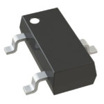 PBRN123ET,215
The activity of extra discounts on wholesale prices is in full swing…
Please fill in your contact information and we will send you the latest wholesale price list.






