ChipApex | Global Electronic Components Supplier
SEARCH
Search Product
Search Post
— IC芯片 | 连接器 | 传感器 | 被动器件 —
Search productSearch post
— IC芯片 | 连接器 | 传感器 | 被动器件 —
Consult the customer manager about the wholesale price.
consultation hotline:86-132-6715-2157
email:[email protected]
Contact the product manager for consultation. One-stop consultation is available.
Do you want a lower wholesale price? Please send us your inquiry and we will reply immediately.
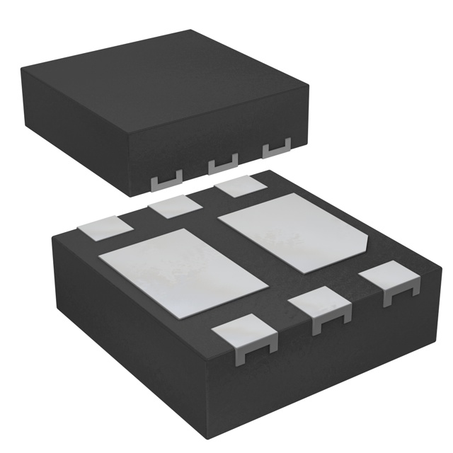
The PBSS4160PANSX is a dual NPN Breakthrough In Small Signal (BISS) transistor manufactured by Nexperia. It features a DFN2020D-6 (SOT1118D) leadless package with visible and solderable side pads. The device supports a collector-emitter voltage of 60 V and a continuous collector current of 1 A per transistor, with a peak pulse current capability of 1.5 A. Key electrical parameters include a maximum collector-base voltage of 60 V, an emitter-base voltage of 7 V, and a typical DC current gain (hFE) ranging from 70 to 430 depending on the collector current. The transition frequency is typically 175 MHz at 50 mA. Total power dissipation reaches 2 W when mounted on a standard FR4 PCB.
Verify the specific ordering suffix against the manufacturer's official documentation to confirm packaging details such as reel or cut tape specifications. Ensure that the component marking code matches the datasheet requirements for quality assurance. Confirm RoHS compliance status through the latest product data sheet before finalizing procurement orders.
Select this component for designs requiring low saturation voltage and high current density in a compact surface-mount footprint. Consider the exposed pad thermal performance when designing the PCB copper area. Verify that the required switching speed and current gain meet the specific circuit demands under expected operating temperatures.
This part belongs to the PBSS4160 series of low VCEsat BISS transistors. It serves as the NPN/NPN configuration within the family, complemented by the PNP/PNP variant PBSS5160PAPS and the NPN/PNP version PBSS4160PANPS. All variants share similar electrical characteristics but differ in internal transistor polarity configurations.
Direct replacements include PBSS4160PANPS (NPN/PNP) and PBSS5160PAPS (PNP/PNP). Verify pin compatibility and polarity requirements before substitution. Other packages in the series may require schematic adjustments due to different pinout arrangements.
 PBSS4160PANSX
The activity of extra discounts on wholesale prices is in full swing…
Please fill in your contact information and we will send you the latest wholesale price list.